JAJSCK8B October 2016 – February 2022 CSD13385F5
PRODUCTION DATA
5.3 Typical MOSFET Characteristics
TA = 25°C (unless otherwise stated)
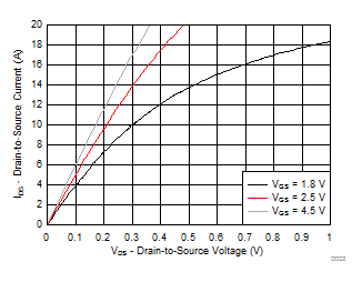 Figure 5-1 Saturation Characteristics
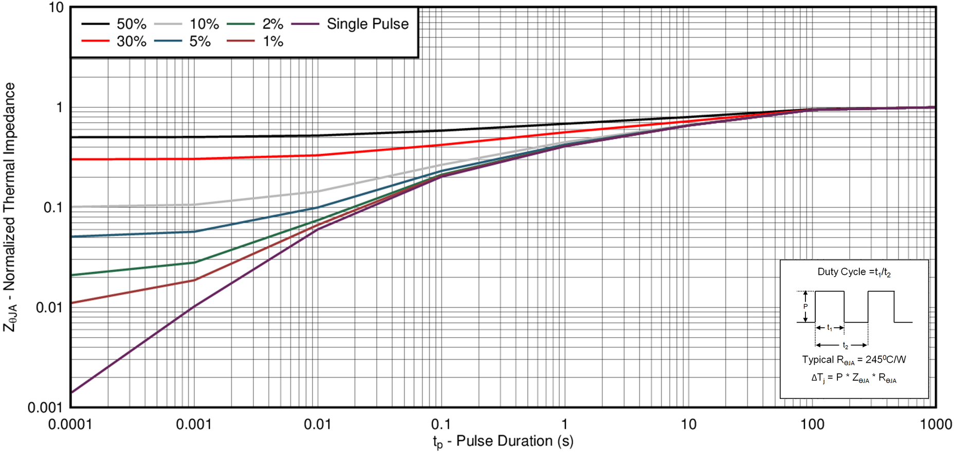 Figure 5-3 Transient Thermal Impedance
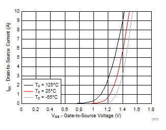
| VDS = 5 V | ||
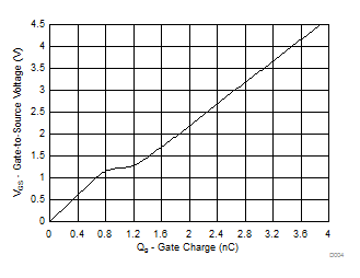
| ID = 0.9 A | VDS = 6 V | |
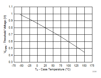
| ID = 250 µA | ||
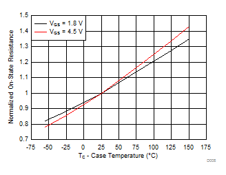
| ID = 0.9 A | ||
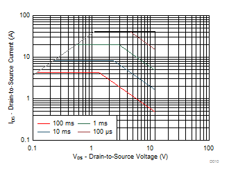
| Single pulse, typical RθJA = 290°C/W | ||
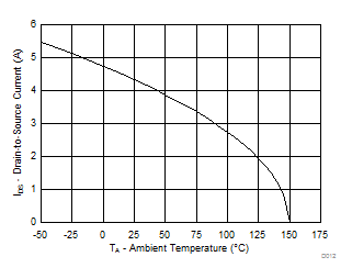
| Typical RθJA = 245°C/W | ||
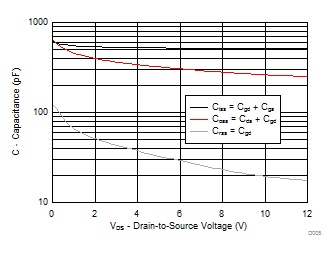 Figure 5-5 Capacitance
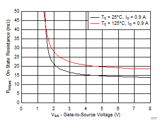 Figure 5-7 On-State Resistance vs Gate-to-Source Voltage
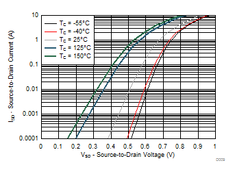 Figure 5-9 Typical Diode Forward Voltage
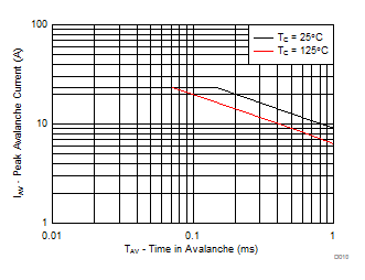 Figure 5-11 Single Pulse Unclamped Inductive Switching