SLPS432C November 2012 – January 2015 CSD16556Q5B
PRODUCTION DATA.
- 1Features
- 2Applications
- 3Description
- 4Revision History
- 5Specifications
- 6Device and Documentation Support
- 7Mechanical, Packaging, and Orderable Information
パッケージ・オプション
デバイスごとのパッケージ図は、PDF版データシートをご参照ください。
メカニカル・データ(パッケージ|ピン)
- DNK|8
サーマルパッド・メカニカル・データ
発注情報
2 Applications
- Point-of-Load Synchronous Buck in Networking, Telecom, and Computing Systems
- Optimized for Synchronous FET Applications
3 Description
This 25 V, 0.9 mΩ, 5 × 6 mm SON NexFET™ power MOSFET is designed to minimize losses in synchronous rectification and other power conversion applications.
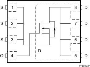
Top View
Product Summary
| TA = 25°C | TYPICAL VALUE | UNIT | ||
|---|---|---|---|---|
| VDS | Drain-to-Source Voltage | 25 | V | |
| Qg | Gate Charge Total (4.5 V) | 36 | nC | |
| Qgd | Gate Charge Gate-to-Drain | 12 | nC | |
| RDS(on) | Drain-to-Source On-Resistance | VGS = 4.5 V | 1.2 | mΩ |
| VGS = 10 V | 0.9 | mΩ | ||
| VGS(th) | Threshold Voltage | 1.4 | V | |
Ordering Information(1)
| Device | Media | Qty | Package | Ship |
|---|---|---|---|---|
| CSD16556Q5B | 13-Inch Reel | 2500 | SON 5 x 6 mm Plastic Package | Tape and Reel |
| CSD16556Q5BT | 7-Inch Reel | 250 |
- For all available packages, see the orderable addendum at the end of the data sheet.
Absolute Maximum Ratings
| TA = 25°C | VALUE | UNIT | |
|---|---|---|---|
| VDS | Drain-to-Source Voltage | 25 | V |
| VGS | Gate-to-Source Voltage | ±20 | V |
| ID | Continuous Drain Current (Package limited) | 100 | A |
| Continuous Drain Current (Silicon limited), TC = 25°C | 263 | ||
| Continuous Drain Current(1) | 40 | A | |
| IDM | Pulsed Drain Current(2) | 400 | A |
| PD | Power Dissipation(1) | 3.2 | W |
| Power Dissipation, TC = 25°C | 191 | ||
| TJ, Tstg |
Operating Junction and Storage Temperature Range |
–55 to 150 | °C |
| EAS | Avalanche Energy, single pulse ID = 103 A, L = 0.1 mH, RG = 25 Ω |
530 | mJ |
RDS(on) vs VGS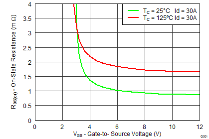 |
Gate Charge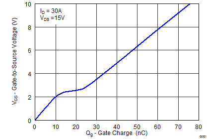 |