JAJSDP2C April 2016 – February 2022 CSD17382F4
PRODUCTION DATA
- 1特長
- 2アプリケーション
- 3概要
- 4Revision History
- 5Specifications
- 6Device and Documentation Support
- 7Mechanical, Packaging, and Orderable Information
パッケージ・オプション
デバイスごとのパッケージ図は、PDF版データシートをご参照ください。
メカニカル・データ(パッケージ|ピン)
- YJC|3
サーマルパッド・メカニカル・データ
発注情報
7.1 Mechanical Dimensions
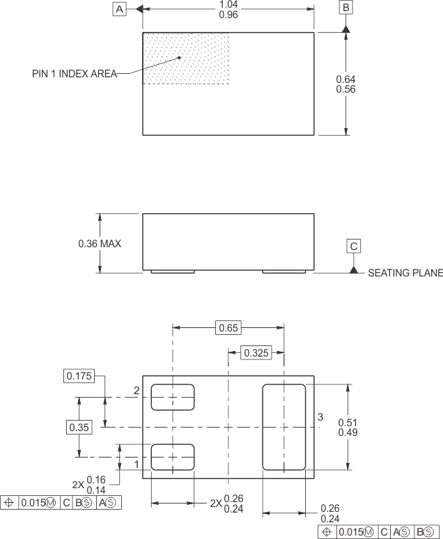
All linear dimensions are in
millimeters. Any dimensions in parenthesis are for reference only. Dimensioning
and tolerancing per ASME Y14.5M.
This drawing is subject to change
without notice.
This package is a Pb-free bump
design. Bump finish may vary. To determine the exact finish, refer to the device
datasheet or contact a local TI representative.