SLPS553 October   2015 CSD19532KTT

PRODUCTION DATA.  

  1. 1Features
  2. 2Applications
  3. 3Description
  4. 4Revision History
  5. 5Specifications
    1. 5.1 Electrical Characteristics
    2. 5.2 Thermal Information
    3. 5.3 Typical MOSFET Characteristics
  6. 6Device and Documentation Support
    1. 6.1 Community Resources
    2. 6.2 Trademarks
    3. 6.3 Electrostatic Discharge Caution
    4. 6.4 Glossary
  7. 7Mechanical, Packaging, and Orderable Information
    1. 7.1 KTT Package Dimensions
    2. 7.2 Recommended PCB Pattern
    3. 7.3 Recommended Stencil Opening (0.125 mm Stencil Thickness)

パッケージ・オプション

デバイスごとのパッケージ図は、PDF版データシートをご参照ください。

メカニカル・データ(パッケージ|ピン)
  • KTT|2
サーマルパッド・メカニカル・データ
発注情報

5 Specifications

5.1 Electrical Characteristics

(TA = 25°C unless otherwise stated)
PARAMETER TEST CONDITIONS MIN TYP MAX UNIT
STATIC CHARACTERISTICS
BVDSS Drain-to-source voltage VGS = 0 V, ID = 250 μA 100 V
IDSS Drain-to-source leakage current VGS = 0 V, VDS = 80 V 1 μA
IGSS Gate-to-source leakage current VDS = 0 V, VGS = 20 V 100 nA
VGS(th) Gate-to-source threshold voltage VDS = VGS, ID = 250 μA 2.2 2.6 3.2 V
RDS(on) Drain-to-source on resistance VGS = 6 V, ID = 90 A 5.3 6.6
VGS = 10 V, ID = 90 A 4.6 5.6
gfs Transconductance VDS = 10 V, ID = 90 A 113 S
DYNAMIC CHARACTERISTICS
Ciss Input capacitance VGS = 0 V, VDS = 50 V, ƒ = 1 MHz 3890 5060 pF
Coss Output capacitance 674 876 pF
Crss Reverse transfer capacitance 14 18 pF
RG Series gate resistance 1.3 2.6 Ω
Qg Gate charge total (10 V) VDS = 50 V, ID = 90 A 44 57 nC
Qgd Gate charge gate to drain 5.6 nC
Qgs Gate charge gate to source 17 nC
Qg(th) Gate charge at Vth 9.6 nC
Qoss Output charge VDS = 50 V, VGS = 0 V 124 nC
td(on) Turn on delay time VDS = 50 V, VGS = 10 V,
IDS = 90 A, RG = 0 Ω
9 ns
tr Rise time 3 ns
td(off) Turn off delay time 14 ns
tf Fall time 2 ns
DIODE CHARACTERISTICS
VSD Diode forward voltage ISD = 90 A, VGS = 0 V 0.9 1.0 V
Qrr Reverse recovery charge VDS= 50 V, IF = 90 A,
di/dt = 300 A/μs
326 nC
trr Reverse recovery time 74 ns

5.2 Thermal Information

(TA = 25°C unless otherwise stated)
THERMAL METRIC MIN TYP MAX UNIT
RθJC Junction-to-case thermal resistance 0.6 °C/W
RθJA Junction-to-ambient thermal resistance 62 °C/W

5.3 Typical MOSFET Characteristics

(TA = 25°C unless otherwise stated)
CSD19532KTT D001_SLPS553.png
Figure 1. Transient Thermal Impedance
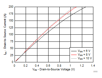
CSD19532KTT D002_SLPS553.gif
Figure 2. Saturation Characteristics
CSD19532KTT D003_SLPS553.gif
VDS = 5 V
Figure 3. Transfer Characteristics
CSD19532KTT D004_SLPS553.gif
VDS = 50 V ID = 90 A
Figure 4. Gate Charge
CSD19532KTT D006_SLPS553.gif
ID = 250 µA
Figure 6. Threshold Voltage vs Temperature
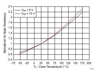
CSD19532KTT D008_SLPS553.gif
ID = 90 A
Figure 8. Normalized On-State Resistance vs Temperature
CSD19532KTT D010_SLPS553.gif
Single Pulse, Max RθJC = 0.6°C/W
Figure 10. Maximum Safe Operating Area
CSD19532KTT D012_SLPS553.gif
Figure 12. Maximum Drain Current vs Temperature
CSD19532KTT D005_SLPS553.gif
Figure 5. Capacitance
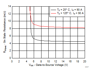
CSD19532KTT D007_SLPS553.gif
Figure 7. On-State Resistance vs Gate-to-Source Voltage
CSD19532KTT D009_SLPS553.gif
Figure 9. Typical Diode Forward Voltage
CSD19532KTT D011_SLPS553.gif
Figure 11. Single Pulse Unclamped Inductive Switching