SLPS584B December 2015 – December 2017 CSD95377Q4M
PRODUCTION DATA.
- 1 Features
- 2 Applications
- 3 Description
- 4 Revision History
- 5 Pin Configuration and Functions
- 6 Specifications
- 7 Detailed Description
- 8 Application and Implementation
- 9 Layout
- 10Device and Documentation Support
- 11Mechanical, Packaging, and Orderable Information
パッケージ・オプション
デバイスごとのパッケージ図は、PDF版データシートをご参照ください。
メカニカル・データ(パッケージ|ピン)
- DPC|8
サーマルパッド・メカニカル・データ
発注情報
1 Features
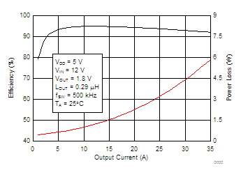
- Above 94% System Efficiency at 15 A
- Max Rated Continuous Current 35 A
- High-Frequency Operation (up to 2 MHz)
- High-Density SON 3.5-mm × 4.5-mm Footprint
- Ultra-Low Inductance Package
- System-Optimized PCB Footprint
- 3.3-V and 5-V PWM Signal Compatible
- Diode Emulation Mode With Forced Continuous Conduction Mode (FCCM)
- Input Voltages to 16 V
- Tri-State PWM Input
- Integrated Bootstrap Diode
- Shoot-Through Protection
- RoHS Compliant – Lead Free Terminal Plating
- Halogen Free
2 Applications
- Point-of-Load Synchronous Buck in Server, Networking, Telecom Systems
- Multiphase Vcore, DDR, and Graphics Solutions
3 Description
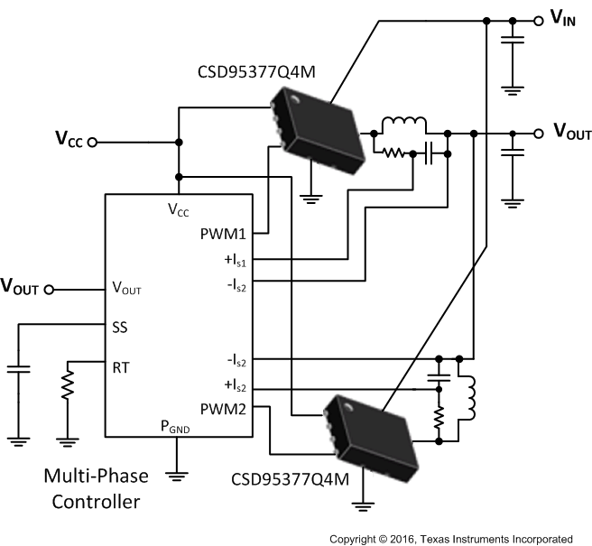
The CSD95377Q4M NexFET™ power stage is a highly-optimized design for use in a high power, high density synchronous buck converter. This product integrates the driver IC and power MOSFETs to complete the power stage switching function. The driver IC has built-in selectable diode emulation function enables Discontinuous Conduction Mode (DCM) operation to improve light load efficiency. This combination produces high-current, high-efficiency, and high-speed switching capability in a small 3.5 mm × 4.5 mm outline package. In addition, the PCB footprint has been optimized to help reduce design time and simplify the completion of the overall system design.
Device Information(1)
| DEVICE | MEDIA | QTY | PACKAGE | SHIP |
|---|---|---|---|---|
| CSD95377Q4M | 13-Inch Reel | 2500 | SON 3.50-mm × 4.50-mm Plastic Package |
Tape and Reel |
| CSD95377Q4MT | 7-Inch Reel | 250 |
- For all available packages, see the orderable addendum at the end of the data sheet.

