JAJSEE6A June 2017 – January 2018 CSD95495QVM
PRODUCTION DATA.
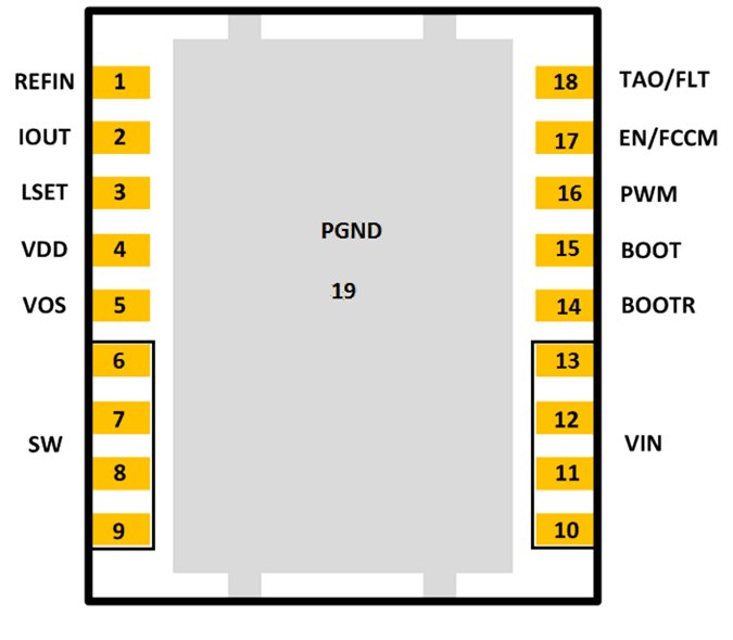
5 Pin Configuration and Functions
Top View

Pin Functions
| PIN | DESCRIPTION | |
|---|---|---|
| NAME | NO. | |
| REFIN | 1 | External reference voltage input for current sensing amplifier. |
| IOUT | 2 | Output of current sensing amplifier. V(IOUT) – V(REFIN) is proportional to the phase current. |
| LSET | 3 | A resistor from this pin to PGND pin sets the inductor value for the internal current sensing circuitry. |
| VDD | 4 | Supply voltage for gate drivers and internal circuitry. |
| VOS | 5 | Output voltage sensing pin for the internal current sensing circuitry. |
| SW | 6-9 | Phase node connecting the HS MOSFET source and LS MOSFET drain – pin connection to the output inductor. |
| VIN | 10-13 | Input voltage pin. Connect input capacitors close to this pin. |
| BOOTR | 14 | Return path for HS gate driver. It is connected to VSW internally. |
| BOOT | 15 | Bootstrap capacitor connection. Connect a minimum 0.1-µF, 16-V, X5R ceramic cap from BOOT to BOOTR pins. The bootstrap capacitor provides the charge to turn on the control FET. The bootstrap diode is integrated. |
| PWM | 16 | Tri-state input from external controller. Logic low sets control FET gate low and sync FET gate high. Logic high sets control FET gate high and sync FET gate low. Both MOSFET gates are set low if PWM stays in Hi-Z for greater than the tri-state shutdown holdoff time (t3HT). |
| EN/FCCM | 17 | This dual function pin either enables the diode emulation function or can be used as a simple enable for the device. When this pin is driven into the tri-state window and held there for more than the tri-state holdoff time, Diode Emulation Mode is enabled for sync FET. When the pin is high, device operates in Forced Continuous Conduction Mode. When the pin is low, both FETs are held off. An internal resistor pulls this pin low if left floating. |
| TAO/FAULT | 18 | Temperature Amplifier Output. Reports a voltage proportional to the IC temperature. An ORing diode is integrated in the IC. When used in multiphase application, a single wire can be used to connect the TAO pins of all the ICs. Only the highest temperature will be reported. TAO will be pulled up to 3.3 V if thermal shutdown, LSOC, or HSS detection circuit is tripped. |
| PGND | 19 | Power ground. |