-
DAC102S085 10-Bit Micro Power DUAL Digital-to-Analog Converter With Rail-to-Rail Output
- 1 Features
- 2 Applications
- 3 Description
- 4 Revision History
- 5 Description (continued)
- 6 Pin Configuration and Functions
- 7 Specifications
- 8 Detailed Description
- 9 Application and Implementation
- 10Power Supply Recommendations
- 11Layout
- 12Device and Documentation Support
- 13Mechanical, Packaging, and Orderable Information
- IMPORTANT NOTICE
パッケージ・オプション
メカニカル・データ(パッケージ|ピン)
サーマルパッド・メカニカル・データ
- DSC|10
発注情報
DAC102S085 10-Bit Micro Power DUAL Digital-to-Analog Converter With Rail-to-Rail Output
1 Features
- Ensured Monotonicity
- Low Power Operation
- Rail-to-Rail Voltage Output
- Power-On Reset to 0 V
- Simultaneous Output Updating
- Wide Power Supply Range (2.7 V to 5.5 V)
- Industry's Smallest Package
- Power Down Modes
- Key Specifications
- Resolution: 10 Bits
- INL: ±2 LSB (Maximum)
- DNL: +0.35 or –0.25 LSB (Maximum)
- Settling Time: 6 µs (Maximum)
- Zero Code Error: 15 mV (Maximum)
- Full-Scale Error: –0.75% FS (Maximum)
- Supply Power
- Normal: 0.6 mW at 3 V, 1.6 mW at 5 V (Typical)
- Power Down: 0.3 µW at 3 V, 0.8 µW at 5 V (Typical)
2 Applications
- Battery-Powered Instruments
- Digital Gain and Offset Adjustment
- Programmable Voltage and Current Sources
- Programmable Attenuators
3 Description
The DAC102S085 is a full-featured, general-purpose DUAL 10-bit voltage-output digital-to-analog converter (DAC) that can operate from a single 2.7-V to 5.5-V supply and consumes 0.6 mW at 3 V and 1.6 mW at 5 V. The DAC102S085 is packaged in 10-pin WSON and VSSOP packages. The 10-pin WSON package makes the DAC102S085 the smallest DUAL DAC in its class. The on-chip output amplifier allows rail-to-rail output swing and the three wire serial interface operates at clock rates up to 40 MHz over the entire supply voltage range. Competitive devices are limited to 25-MHz clock rates at supply voltages in the 2.7-V to 3.6-V range. The serial interface is compatible with standard SPI™, QSPI, MICROWIRE and DSP interfaces.
The reference for the DAC102S085 serves both channels and can vary in voltage between 1 V and VA, providing the widest possible output dynamic range. The DAC102S085 has a 16-bit input shift register that controls the outputs to be updated, the mode of operation, the power-down condition, and the binary input data. Both outputs can be updated simultaneously or individually depending on the setting of the two mode of operation bits.
Device Information(1)
| PART NUMBER | PACKAGE | BODY SIZE (NOM) |
|---|---|---|
| DAC102S085 | VSSOP (10) | 3.00 mm × 3.00 mm |
| WSON (10) | 3.00 mm × 3.00 mm |
- For all available packages, see the orderable addendum at the end of the data sheet.
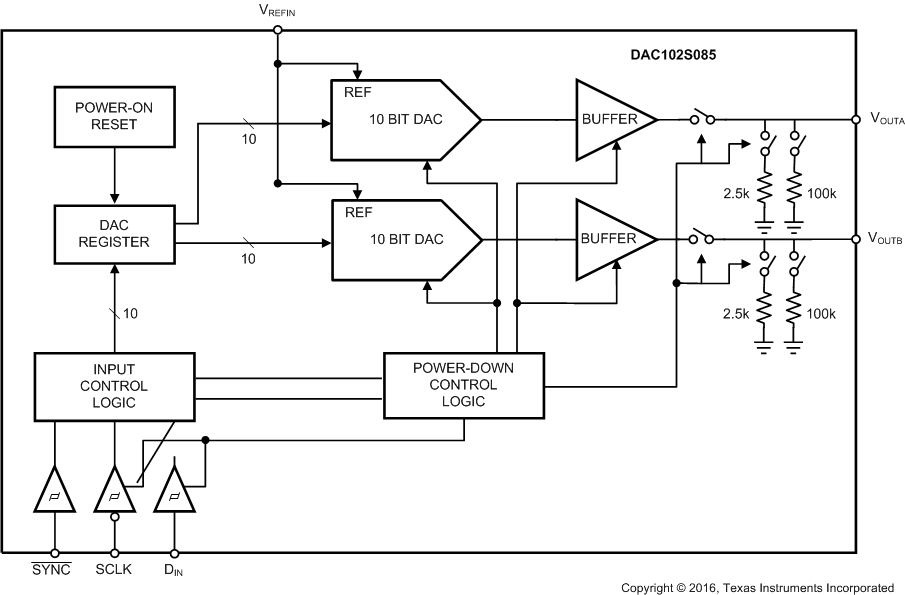
Block Diagram

4 Revision History
Changes from E Revision (March 2013) to F Revision
- Added ESD Ratings table, Feature Description section, Device Functional Modes, Application and Implementation section, Power Supply Recommendations section, Layout section, Device and Documentation Support section, and Mechanical, Packaging, and Orderable Information section.Go
Changes from D Revision (March 2013) to E Revision
- Changed layout of National Data Sheet to TI formatGo
5 Description (continued)
A power-on reset circuit ensures that the DAC output powers up to zero volts and remains there until there is a valid write to the device. A power-down feature reduces power consumption to less than a microWatt with three different termination options.
The low power consumption and small packages of the DAC102S085 make it an excellent choice for use in battery-operated equipment.
The DAC102S085 is one of a family of pin compatible DACs, including the 8-bit DAC084S085 and the 12-bit DAC122S085. The DAC102S085 operates over the extended industrial temperature range of −40°C to 105°C.
6 Pin Configuration and Functions


Pin Functions
| PIN | TYPE | DESCRIPTION | |
|---|---|---|---|
| NO. | NAME | ||
| 1 | VA | Supply | Power supply input. Must be decoupled to GND. |
| 2 | VOUTA | Analog Output | Channel A Analog Output Voltage. |
| 3 | VOUTB | Analog Output | Channel B Analog Output Voltage. |
| 4, 5 | NC | — | Not Connected |
| 6 | GND | Ground | Ground reference for all on-chip circuitry. |
| 7 | VREFIN | Analog Input | Unbuffered reference voltage shared by all channels. Must be decoupled to GND. |
| 8 | DIN | Digital Input | Serial Data Input. Data is clocked into the 16-bit shift register on the falling edges of SCLK after the fall of SYNC. |
| 9 | SYNC | Digital Input | Frame synchronization input for the data input. When this pin goes low, it enables the input shift register and data is transferred on the falling edges of SCLK. The DAC is updated on the 16th clock cycle unless SYNC is brought high before the 16th clock, in which case the rising edge of SYNC acts as an interrupt and the write sequence is ignored by the DAC. |
| 10 | SCLK | Digital Input | Serial Clock Input. Data is clocked into the input shift register on the falling edges of this pin. |
| 11 | PAD(1) | Ground | Exposed die attach pad can be connected to ground or left floating. Soldering the pad to the PCB offers optimal thermal performance and enhances package self-alignment during reflow. |