SNAS410F May 2008 – July 2016 DAC121S101QML-SP
PRODUCTION DATA.
- 1 Features
- 2 Applications
- 3 Description
- 4 Revision History
- 5 Pin Configuration and Functions
-
6 Specifications
- 6.1 Absolute Maximum Ratings
- 6.2 ESD Ratings
- 6.3 Recommended Operating Conditions
- 6.4 Thermal Information
- 6.5 DAC121S101QML-SP Electrical Characteristics DC Parameters
- 6.6 DAC121S101QML-SP Electrical Characteristics AC and Timing Characteristics
- 6.7 DAC121S101QML Electrical Characteristics Radiation Electrical Characteristics
- 6.8 DAC121S101QML-SP Electrical Characteristics Operating Life Test Delta Parameters TA at 25°C
- 6.9 Typical Characteristics
- 7 Detailed Description
- 8 Application and Implementation
- 9 Power Supply Recommendations
- 10Layout
- 11Device and Documentation Support
- 12Mechanical, Packaging, and Orderable Information
7 Detailed Description
7.1 Overview
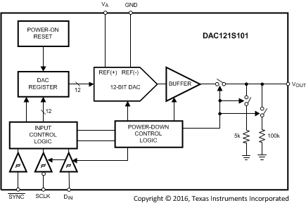
The DAC121S101QML-SP device is a full-featured, general purpose 12-bit voltage-output digital-to-analog converter (DAC). Control of the output of the DAC is achieved over a 3-wire SPI interface. Once the DAC output has been set, additional communication with the DAC is not required unless the output condition needs to be changed. Likewise, the DAC121S101QML-SP power-on state is 0 V. The DAC output will remain at 0 V until a valid write sequence is made.
7.2 Functional Block Diagram

7.3 Feature Description
7.3.1 DAC Section
The DAC121S101QML-SP is fabricated on a CMOS process with an architecture that consists of switches and a resistor string that are followed by an output buffer. The power supply serves as the reference voltage. The input coding is straight binary with an ideal output voltage of:
where
- D is the decimal equivalent of the binary code that is loaded into the DAC register and can take on any value between 0 and 4095.
7.3.2 Resistor String
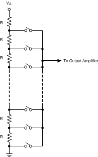
Figure 30 shows the simplified resistor string. Conceptually, this string consists of 4096 equal valued resistors with a switch at each junction of two resistors, plus a switch to ground. The code loaded into the DAC register determines which switch is closed, connecting the proper node to the amplifier. This configuration ensures that the DAC is monotonic.
 Figure 30. DAC Resistor String
7.3.3 Output Amplifier
The output buffer amplifier is a rail-to-rail type, providing an output voltage range of 0 V to VA. All amplifiers, even rail-to-rail types, exhibit a loss of linearity as the output approaches the supply rails (0 V and VA, in this case). For this reason, linearity is specified over less than the full output range of the DAC. The output capabilities of the amplifier are described in the electrical tables in Specifications.
7.3.4 Power-On Reset
The power-on reset circuit controls the output voltage during power-up. Upon application of power, the DAC register is filled with zeros and the output voltage is 0 V and remains there until a valid write sequence is made to the DAC.
7.4 Device Functional Modes
7.4.1 Power-Down Modes
The DAC121S101QML-SP has four modes of operation. These modes are set with two bits (DB13 and DB12) in the control register.
Table 2. Modes of Operation
| DB13 | DB12 | OPERATING MODE |
| 0 | 0 | Normal Operation |
| 0 | 1 | Power Down with 5 kΩ to GND |
| 1 | 0 | Power Down with 100 kΩ to GND |
| 1 | 1 | Power Down with Hi-Z |
When both DB13 and DB12 are 0, the device operates normally. For the other three possible combinations of these bits the supply current drops to its power-down level and the output is pulled down with either a 5-kΩ or a 100-kΩ resistor, or is in a high impedance state, as described in Table 2.
The bias generator, output amplifier, the resistor string, and other linear circuitry are all shut down in any of the power-down modes. Minimum power consumption is achieved in the power-down mode with SCLK disabled and SYNC and DIN idled low.
7.5 Programming
7.5.1 Serial Interface
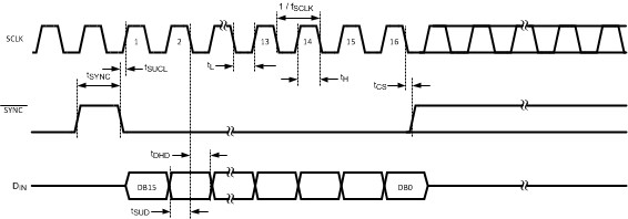
The three-wire interface is compatible with SPI, QSPI, and MICROWIRE, as well as most DSPs. See Figure 31 for information on a write sequence.
A write sequence begins by bringing the SYNC line low. When SYNC is low, the data on the DIN line is clocked into the 16-bit serial input register on the falling edges of SCLK. On the 16th falling clock edge, the last data bit is clocked in and the programmed function (a change in the mode of operation or a change in the DAC register contents) is executed. At this point the SYNC line may be kept low or brought high. In either case, it must be brought high for the minimum specified time before the next write sequence as a falling edge of SYNC can initiate the next write cycle.
Because the SYNC and DIN buffers draw more current when they are high, they must be idled low between write sequences to minimize power consumption.
 Figure 31. DAC121S101QML-SP Timing
7.5.2 Input Shift Register
The input shift register, Figure 32, has 16 bits. The first two bits are don't cares and are followed by two bits that determine the mode of operation (normal mode or one of three power-down modes). The contents of the serial input register are transferred to the DAC register on the sixteenth falling edge of SCLK. See the timing diagram, Figure 31.
 Figure 32. Input Register Contents
Normally, the SYNC line is kept low for at least 16 falling edges of SCLK and the DAC is updated on the 16th SCLK falling edge. However, if SYNC is brought high before the 16th falling edge, the shift register is reset and the write sequence is invalid. The DAC register is not updated and there is no change in the mode of operation or in the output voltage.