SLAS646C December 2009 – May 2015 DAC3282
PRODUCTION DATA.
- 1 Features
- 2 Applications
- 3 Description
- 4 Revision History
- 5 Pin Configuration and Functions
-
6 Specifications
- 6.1 Absolute Maximum Ratings
- 6.2 ESD Ratings
- 6.3 Recommended Operating Conditions
- 6.4 Thermal Information
- 6.5 Electrical Characteristics - DC Specifications
- 6.6 Electrical Characteristics - AC Specifications
- 6.7 Electrical Characteristics - Digital Specifications
- 6.8 Timing Characteristics
- 6.9 Typical Characteristics
-
7 Detailed Description
- 7.1 Overview
- 7.2 Functional Block Diagram
- 7.3
Feature Description
- 7.3.1 Input FIFO
- 7.3.2 FIFO Alarms
- 7.3.3 FIFO Modes of Operation
- 7.3.4 Dual Sync Sources Mode
- 7.3.5 Single Sync Source Mode
- 7.3.6 Bypass Mode
- 7.3.7 Data Pattern Checker
- 7.3.8 FIR Filters
- 7.3.9 Coarse Mixer
- 7.3.10 Digital Offset Control
- 7.3.11 Temperature Sensor
- 7.3.12 Sleep Modes
- 7.3.13 Reference Operation
- 7.4 Device Functional Modes
- 7.5 Programming
- 7.6
Register Maps
- 7.6.1 CONFIG0 (address = 0x00) [reset = 0x70]
- 7.6.2 CONFIG1 (address = 0x01) [reset = 0x11]
- 7.6.3 CONFIG2 (address = 0x02) [reset = 0x00]
- 7.6.4 CONFIG3 (address = 0x03) [reset = 0x10]
- 7.6.5 CONFIG4 (address = 0x04) [reset = 0xFF]
- 7.6.6 CONFIG5 (address = 0x05) READ ONLY
- 7.6.7 CONFIG6 (address =0x06) [reset = 0x00]
- 7.6.8 CONFIG7 (address = 0x07) [reset = 0x00] (WRITE TO CLEAR)
- 7.6.9 CONFIG8 (address = 0x08) [reset = 0x00] (WRITE TO CLEAR)
- 7.6.10 CONFIG9 (address = 0x09) [reset = 0x7A]
- 7.6.11 CONFIG10 (address = 0x0A) [reset = 0xB6]
- 7.6.12 CONFIG11 (address = 0x0B) [reset = 0xEA]
- 7.6.13 CONFIG12 (address =0x0C) [reset = 0x45]
- 7.6.14 CONFIG13 (address =0x0D) [reset = 0x1A]
- 7.6.15 CONFIG14 Register Name (address = 0x0E) [reset = 0x16]
- 7.6.16 CONFIG15 Register Name (address = 0x0F) [reset = 0xAA]
- 7.6.17 CONFIG16 (address = 0x10) [reset = 0xC6]
- 7.6.18 CONFIG17 (address = 0x11) [reset = 0x00]
- 7.6.19 CONFIG18 (address = 0x12) [reset = 0x02]
- 7.6.20 CONFIG19 (address = 0x13) [reset = 0x00]
- 7.6.21 CONFIG20 (address = 0x14) [reset = 0x00] (CAUSES AUTOSYNC)
- 7.6.22 CONFIG21 (address = 0x15) [reset = 0x00]
- 7.6.23 CONFIG22 (address = 0x16) [reset = 0x00]
- 7.6.24 CONFIG23 (address = 0x17) [reset = 0x00]
- 7.6.25 CONFIG24 (address = 0x18) [reset = 0x83]
- 7.6.26 CONFIG25 (address = 0x19) [reset = 0x00]
- 7.6.27 CONFIG26 (address = 0x1A) [reset = 0x00]
- 7.6.28 CONFIG27 (address =0x1B) [reset = 0x00]
- 7.6.29 CONFIG28 (address = 0x1C) [reset = 0x00]
- 7.6.30 CONFIG29 (address = 0x1D) [reset = 0x00]
- 7.6.31 CONFIG30 (address = 0x1E) [reset = 0x00]
- 7.6.32 VERSION31 (address = 0x1F) [reset = 0x43] (READ ONLY)
- 8 Application and Implementation
- 9 Power Supply Recommendations
- 10Layout
- 11Device and Documentation Support
- 12Mechanical, Packaging, and Orderable Information
7 Detailed Description
7.1 Overview
The DAC3282 is a dual-channel 16-bit 800 MSPS digital-to-analog converter (DAC) with an 8-bit LVDS input data bus with on-chip termination, optional 2x-4x interpolation filters, digital IQ compensation and internal voltage reference. Input data can be interpolated by 2x or 4x through on-chip interpolating FIR filters with over 85 dB of stop-band attenuation. Multiple DAC3282 devices can be fully synchronized. The DAC3282 allows either a complex or real output. An optional coarse mixer in complex mode provides frequency upconversion and the dual DAC output produces a complex Hilbert Transform pair. The digital IQ compensation feature allows optimization of phase, gain and offset to maximize sideband rejection and minimize LO feed-through of an external quadrature modulator performing the final single sideband RF up-conversion.
7.2 Functional Block Diagram
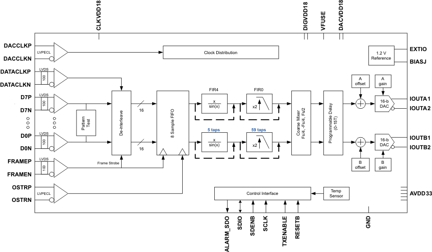
7.3 Feature Description
7.3.1 Input FIFO
The DAC3282 includes a 2-channel, 16-bits wide and 8-samples deep input FIFO which acts as an elastic buffer. The purpose of the FIFO is to absorb any timing variations between the input data and the internal DAC data rate clock such as the ones resulting from clock-to-data variations from the data source.
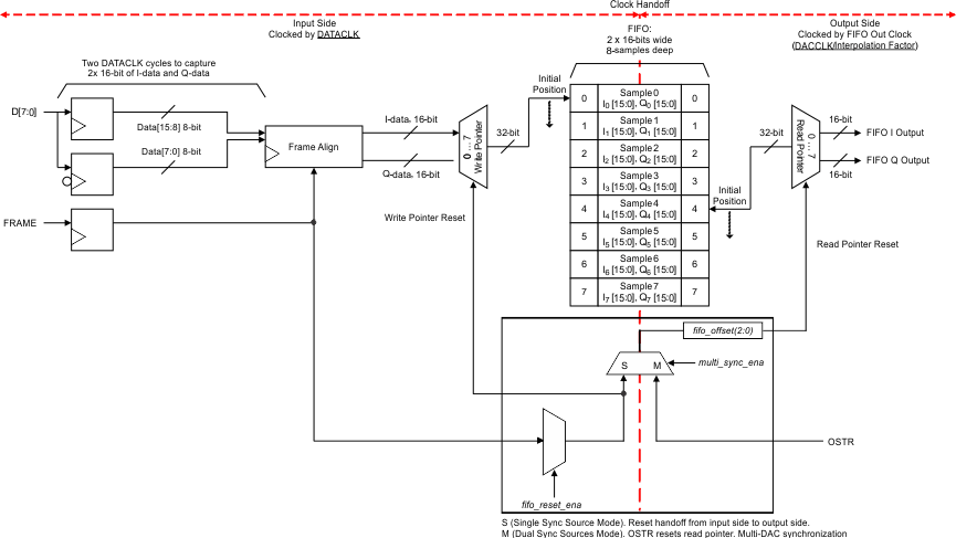
Figure 24 shows the block diagram of the FIFO.
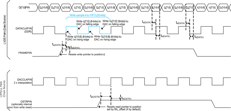
Data is written to the device 8-bits at a time on the rising and falling edges of DATACLK. In order to form a complete 32-bit wide sample (16-bit I-data and 16-bit Q-data) two DATACLK periods are required as shown in Figure 25. Each 32-bit wide sample is written into the FIFO at the address indicated by the write pointer. Similarly, data from the FIFO is read by the FIFO Out Clock 32-bits at a time from the address indicated by the read pointer. The FIFO Out Clock is generated internally from the DACCLK signal and its rate is equal to DACCLK/Interpolation. Each time a FIFO write or FIFO read is done the corresponding pointer moves to the next address.
The reset position for the FIFO read and write pointers is set by default to addresses 0 and 4 as shown in Figure 24. This offset gives optimal margin within the FIFO. The default read pointer location can be set to another value using fifo_offset(2:0) in register CONFIG3. Under normal conditions data is written-to and read-from the FIFO at the same rate and consequently the write and read pointer gap remains constant. If the FIFO write and read rates are different, the corresponding pointers will be cycling at different speeds which could result in pointer collision. Under this condition the FIFO attempts to read and write data from the same address at the same time which will result in errors and thus must be avoided.
The FRAME signal besides acting as a frame indicator can also used to reset the FIFO pointers to their initial location. Unlike Data, the FRAME signal is latched only on the rising edges of DATACLK. When a rising edge occurs on FRAME, the pointers will return to their original position. The write pointer is always set back to position 0 upon reset. The read pointer reset position is determined by fifo_offset (address 4 by default).
Similarly, the read pointer sync source is selected by multi_sync_sel (CONFIG19). Either the FRAME or OSTR signal can be set to reset the read pointer. If FRAME is used to reset the read pointer, the FIFO Out Clock will recapture the FRAME signal to reset the read pointer. This clock domain transfer (DATACLK to FIFO Out Clock) results in phase ambiguity of the reset signal. This limits the precise control of the output timing and makes full synchronization of multiple devices difficult.
To alleviate this, the device offers the alternative of resetting the FIFO read pointer independently of the write pointer by using the OSTR signal. The OSTR signal is sampled by DACCLK and must satisfy the timing requirements in the specification table. In order to minimize the skew it is recommended to use the same clock distribution device such as Texas Instruments CDCE62005 to provide the DACCLK and OSTR signals to all the DAC3282 devices in the system. Swapping the polarity of the DACCLK output with respect to the OSTR output establishes proper phase relationship.
The FIFO pointers reset procedure can be done periodically or only once during initialization as the pointers automatically return to the initial position when the FIFO has been filled. To reset the FIFO periodically, it is necessary to have FRAME and OSTR signals to repeat at multiple of 8 FIFO samples. To disable FIFO reset, set fifo_reset_ena and multi_sync_ena (CONFIG0) to 0.
The frequency limitation for the FRAME signal is the following
fSYNC = fDATACLK/(n x 16) where n = 1, 2,...
The frequency limitation for the OSTR signal is the following:
fOSTR = fDAC/(n x interpolation x 8) where n = 1, 2, ...
The frequencies above are at maximum when n = 1. This is when FRAME and OSTR have a rising edge transition every 8 FIFO samples. The occurrence can be made less frequent by setting n > 1, for example, every n x 8 FIFO samples.
7.3.2 FIFO Alarms
The FIFO only operates correctly when the write and read pointers are positioned properly. If either pointer over or under runs the other, samples will be duplicated or skipped. To prevent this, register CONFIG7 can be used to track three FIFO related alarms:
- alarm_fifo_2away. Occurs when the pointers are within two addresses of each other.
- alarm_fifo_1away. Occurs when the pointers are within one address of each other.
- alarm_fifo_collision. Occurs when the pointers are equal to each other.
These three alarm events are generated asynchronously with respect to the clocks and can be accessed either through CONFIG7 or through the ALARM_SDO pin.
7.3.3 FIFO Modes of Operation
The DAC3282 input FIFO can be completely bypassed through registers config0 and config19. The register configuration for each mode is described in Table 1.
7.3.4 Dual Sync Sources Mode
This is the recommended mode of operation for those applications that require precise control of the output timing. In Dual Sync Sources mode, the FIFO write and read pointers are reset independently. The FIFO write pointer is reset using the LVDS FRAME signal, and the FIFO read pointer is reset using the LVPECL OSTR signal. This allows LVPECL OSTR signal to control the phase of the output for either a single chip or multiple chips. Multiple devices can be fully synchronized in this mode.
7.3.5 Single Sync Source Mode
In Single Sync Source mode, the FIFO write and read pointers are reset from the same LVDS FRAME signal. This mode has a possibility of up to 2 DAC clocks offset between the outputs of multiple devices (the DAC outputs of the same device maintain the phase phase). Applications requiring exact output timing control will need Dual Sync Sources mode instead of Single Sync Source Mode. A rising edge for FIFO and clock divider sync is recommended. Periodic sync signal is not recommended due to non-deterministic latency of the sync signal through the clock domain transfer.
7.3.6 Bypass Mode
In FIFO bypass mode, the FIFO block is not used. As a result the input data is handed off from the DATACLK to the DACCLK domain without any compensation. In this mode the relationship between DATACLK and DACCLK t(align) is critical and used as a synchronizing mechanism for the internal logic. Due to the t(align) constraint it is highly recommended that a clock synchronizer such as Texas Instruments' CDCM7005 or CDCE62005 is used to provide both clock inputs. In bypass mode the pointers have no effect on the data path or handoff.
7.3.7 Data Pattern Checker
The DAC3282 incorporates a simple pattern checker test in order to determine errors in the data interface. The main cause of failure is setup/hold timing issues. The test mode is enabled by asserting iotest_ena in register config1. In test mode the analog outputs are deactivated regardless of the state of TXENABLE.
The data pattern key used for the test is 8 words long and is specified by the contents of iotest_pattern[0:7] in registers config9 through config16. The data pattern key can be modified by changing the contents of these registers.
The first word in the test frame is determined by a rising edge transition in FRAME. At this transition, the pattern0 word should be input to the data pins. Patterns 1 through 7 should follow sequentially on each edge of DATACLK (rising and falling). The sequence should be repeated until the pattern checker test is disabled by setting iotest_ena back to “0”. It is not necessary to have a rising FRAME edge aligned with every pattern0 word, just the first one to mark the beginning of the series.
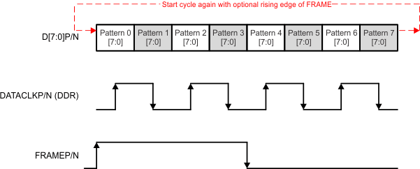 Figure 26. IO Pattern Checker Data Transmission Format
The test mode determines if the 8-bit LVDS data D[7:0]P/N of all the patterns were received correctly by comparing the received data against the data pattern key. If any of the 8-bit data D[7:0]P/N were received incorrectly, the corresponding bits in iotest_results(7:0) in register config8 will be set to “1” to indicate bit error location. Furthermore, the error condition will trigger the alarm_from_iotest bit in register config7 to indicate a general error in the data interface. When data pattern checker mode is enabled, this alarm in register config7, bit 3 is the only valid alarm. Other alarms in register config7 are not valid and can be disregarded.
For instance, pattern0 is programmed to the default of 0x7A. If the received Pattern 0 is 0x7B, then bit 0 in iotest_results(7:0) will be set to “1” to indicate an error in bit 0 location. The alarm_from_iotest will also be set to “1” to report the data transfer error. The user can then narrow down the error from the bit location information and implement the fix accordingly.
The alarms can be cleared by writing 0x00 to iotest_results(7:0) and “0” to alarm_from_iotest through the serial interface. The serial interface will read back 0s if there are no errors or if the errors are cleared. The corresponding alarm bit will remain a “1” if the errors remain.
It is recommended to enable the pattern checker and then run the pattern sequence for 100 or more complete cycles before clearing the iotest_results(7:0) and alarm_from_iotest. This will eliminate the possibility of false alarms generated during the setup sequence.
 Figure 27. DAC3282 Pattern Check Block Diagram
7.3.8 FIR Filters
The DAC3282 has two FIR filters, a 2x interpolation FIR (FIR0) and a non-interpolating FIR (FIR4) that compensates for the sinc droop of the DAC on zero-IF applications. The correction filter is placed before the interpolating filter and can only be used with both FIRs enabled.
Figure 28 shows the magnitude spectrum response for FIR0, a 59-tap interpolating half-band filter. The transition band is from 0.4 to 0.6 × fIN (the input data rate for the FIR filter) with < 0.002dB of pass-band ripple and > 85 dB stop-band attenuation. Figure 29 shows the transition band region from 0.36 to 0.46 × fIN. Up to 0.45 × fIN there is less than 0.5 dB of attenuation.
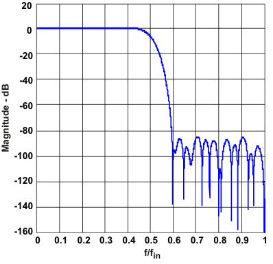 Figure 28. Magnitude Spectrum for FIR0
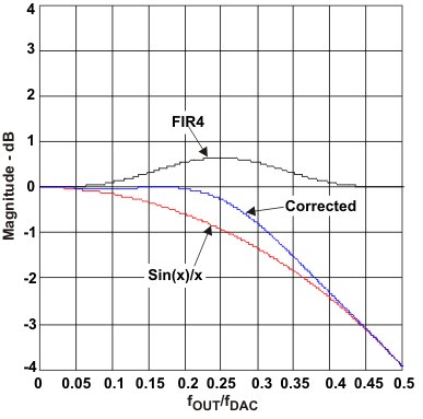 Figure 30. Magnitude Spectrum for Zero-IF Sinc
Correction Filter up to 0.5 × fDAC
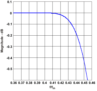 Figure 29. FIR0 Transition Band
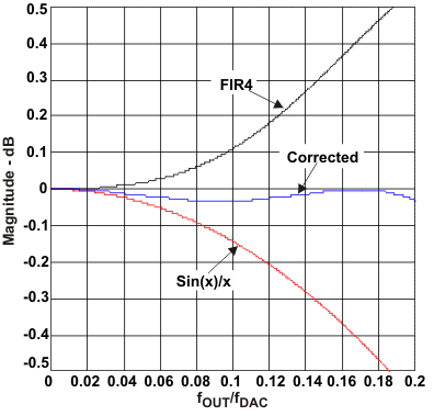 Figure 31. Correction Range of Zero-IF Sinc
 Correction Filter 0 to 0.2 × fDAC
The DAC sample and hold operation results in the well known sin(x)/x or sinc(x) frequency response shown in Figure 30 (red line). The DAC3282 has a 5-tap inverse sinc filter (FIR4) placed before the 2x interpolation filter to compensate for this effect up to 0.2 × fDAC. The inverse sinc filter runs at the input data rate and is operational only if the 2x interpolation filter is enabled as well, correspondingly the rate of this filter is always half of the DAC update rate. As a result, the filter cannot completely flatten the frequency response of the sample and hold output as shown in Figure 30.
Figure 31 shows the magnitude spectrum for FIR4 over the correction range. The inverse sinc filter response (Figure 31, black line) has approximately the opposite frequency response to sin(x)/x between 0 to 0.2 x fDAC, resulting in the corrected response in Figure 31 (blue line). Between 0 to 0.2 × fDAC, the inverse sinc filter compensates for the sample and hold roll-off with less than 0.04-dB error.
The filter taps for all digital filters are listed in Table 2.
Table 2. FIR Filter Coefficients
| FIR0 2x Interpolating Half-Band Filter |
FIR4 Non-Interpolating Zero-IF Sinc Correction Filter |
|
|---|---|---|
| 59 Taps | 5 Taps | |
| 4 | 4 | 1 |
| 0 | 0 | –5 |
| –12 | –12 | 264(1) |
| 0 | 0 | –5 |
| 28 | 28 | 1 |
| 0 | 0 | |
| –58 | –58 | |
| 0 | 0 | |
| 108 | 108 | |
| 0 | 0 | |
| –188 | –188 | |
| 0 | 0 | |
| 308 | 308 | |
| 0 | 0 | |
| –483 | –483 | |
| 0 | 0 | |
| 734 | 734 | |
| 0 | 0 | |
| –1091 | –1091 | |
| 0 | 0 | |
| 1607 | 1607 | |
| 0 | 0 | |
| –2392 | –2392 | |
| 0 | 0 | |
| 3732 | 3732 | |
| 0 | 0 | |
| –6681 | –6681 | |
| 0 | 0 | |
| 20768 | 20768 | |
| 32768(1) | ||
The zero-IF sinc filter has a gain > 1 at all frequencies. Therefore, the input data must be reduced from full scale to prevent saturation in the filter. The amount of back-off required depends on the signal frequency, and is set such that at the signal frequencies the combination of the input signal and filter response is less than 1 (0 dB). For example, if the signal input to FIR4 is at 0.1 × fDAC, the response of FIR4 is 0.1 dB, and the signal must be backed off from full scale by 0.1 dB to avoid saturation.
Note that the loss of signal amplitude may result in lower SNR due to decrease in signal amplitude.
7.3.9 Coarse Mixer
The DAC3282 has a coarse mixer block capable of shifting the input signal spectrum by the fixed mixing frequencies fS/2 or ±fS/4. The coarse mixing function is built into the interpolation filter and thus FIR0 must be enabled to use it.
Treating channels A and B as a complex vector of the form I(t) + j Q(t), where I(t) = A(t) and Q(t) = B(t), the outputs of the coarse mixer, AOUT(t) and BOUT(t) are equivalent to:


where fCMIX is the fixed mixing frequency selected by mixer_func(1:0). For fS/2, +fS/4 and –fS/4 the above operations result in the simple mixing sequences shown in Table 3.
Table 3. Coarse Mixer Sequences
| Mode | mixer_func(1:0) | Mixing Sequence |
|---|---|---|
| Normal (Low Pass, No Mixing) |
00 | AOUT = { +A, +A , +A, +A } BOUT = { +B, +B , +B, +B } |
| fS/2 | 01 | AOUT = { +A, –A , +A, –A } BOUT = { +B, –B , +B, –B } |
| +fS/4 | 10 | AOUT = { +A, –B , –A, +B } BOUT = { +B, +A , –B, –A } |
| –fS/4 | 11 | AOUT = { +A, +B , –A, –B } BOUT = { +B, –A , –B, +A } |
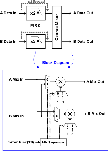 Figure 32. Coarse Mixers Block Diagram
The coarse mixer in the DAC3282 treats the A and B inputs as complex input data and for most mixing frequencies produces a complex output. Only when the mixing frequency is set to fS/2 the A and B channels can be maintained isolated as shown in Table 3. In this case the two channels are upconverted as independent signals. By setting the mixer to fS/2 the FIR0 outputs are inverted thus behaving as a high-pass filter.
Table 4. Dual-Channel Real Upconversion Options
| FIR Mode | Input Frequency(1) | Output Frequency(1) | Signal Bandwidth(1) | Spectrum Inverted? |
|---|---|---|---|---|
| Low pass | 0.0 to 0.4 x fDATA | 0.0 to 0.4 x fDATA | 0.4 x fDATA | No |
| High pass | 0.0 to 0.4 x fDATA | 0.6 to 1.0 x fDATA | 0.4 x fDATA | Yes |
7.3.10 Digital Offset Control
The qmc_offseta(12:0) and qmc_offsetb(12:0) values in registers CONFIG20 through CONFIG23 can be used to independently adjust the A and B path DC offsets. Both offset values are in represented in 2s-complement format with a range from –4096 to 4095.
Note that a write to register CONFIG20 is required to load the values of all four qmc_offset registers (CONFIG20-CONFIG23) into the offset block simultaneously. When updating the offset values CONFIG20 should be written last. Programming any of the other three registers will not affect the offset setting.
The offset value adds a digital offset to the digital data before digital-to-analog conversion. Since the offset is added directly to the data it may be necessary to back off the signal to prevent saturation. Both data and offset values are LSB aligned.
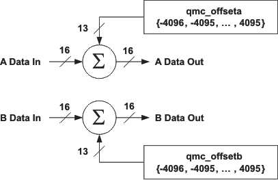 Figure 33. Digital Offset Block Diagram
7.3.11 Temperature Sensor
The DAC3282 incorporates a temperature sensor block which monitors the temperature by measuring the voltage across 2 transistors. The voltage is converted to an 8-bit digital word using a successive-approximation (SAR) analog to digital conversion process. The result is scaled, limited and formatted as a twos complement value representing the temperature in degrees Celsius.
The sampling is controlled by the serial interface signals SDENB and SCLK. If the temperature sensor is enabled (tsense_ena = 1 in register CONFIG24) a conversion takes place each time the serial port is written or read. The data is only read and sent out by the digital block when the temperature sensor is read in register CONFIG5. The conversion uses the first eight clocks of the serial clock as the capture and conversion clock, the data is valid on the falling eighth SCLK. The data is then clocked out of the chip on the rising edge of the ninth SCLK. No other clocks to the chip are necessary for the temperature sensor operation. As a result the temperature sensor is enabled even when the device is in sleep mode.
In order for the process described above to operate properly, the serial port read from CONFIG5 must be done with an SCLK period of at least 1 µs. If this is not satisfied the temperature sensor accuracy is greatly reduced.
7.3.12 Sleep Modes
The DAC3282 features independent sleep control of each DAC (sleepa and sleepb), their corresponding clock path (clkpath_sleep_a and clkpath_sleep_b) as well as the clock input receiver of the device (clkrecv_sleep). The sleep control of each of these components is done through the SIF interface and is enabled by setting a 1 to the corresponding sleep register.
Complete power down of the device is set by setting all of these components to sleep. Under this mode the supply power consumption is reduced to 15mW. Power-up time in this case will be in the milliseconds range. Alternatively for those applications were power-up and power-down times are critical it is recommended to only set the DACs to sleep through the sleepa and sleepb registers. In this case both the sleep and wake-up times are only 90µs.
7.3.13 Reference Operation
The DAC3282 uses a bandgap reference and control amplifier for biasing the full-scale output current. The full-scale output current is set by applying an external resistor RBIAS to pin BIASJ. The bias current IBIAS through resistor RBIAS is defined by the on-chip bandgap reference voltage and control amplifier. The default full-scale output current equals 16 times this bias current and can thus be expressed as:
IOUTFS = 16 × IBIAS = 16 × VEXTIO / RBIAS
Each DAC has a 4-bit independent coarse gain control via coarse_daca(3:0) and coarse_dacb (3:0) in the CONFIG4 register. Using gain control, the IOUTFS can be expressed as:
IOUTAFS = (DACA_gain + 1) × IBIAS = (DACA_gain + 1) × VEXTIO / RBIAS
IOUTBFS = (DACB_gain + 1) × IBIAS = (DACB_gain + 1) × VEXTIO / RBIAS
Where VEXTIO is the voltage at terminal EXTIO. The bandgap reference voltage delivers an accurate voltage of 1.2V. This reference is active when extref_ena = ‘0’ in CONFIG25. An external decoupling capacitor CEXT of 0.1 μF should be connected externally to terminal EXTIO for compensation. The bandgap reference can additionally be used for external reference operation. In that case, an external buffer with high impedance input should be applied in order to limit the bandgap load current to a maximum of 100 nA. The internal reference can be disabled and overridden by an external reference by setting the CONFIG25 extref_ena control bit. Capacitor CEXT may hence be omitted. Terminal EXTIO thus serves as either input or output node.
The full-scale output current can be adjusted from 20 mA down to 2 mA by varying resistor RBIAS or changing the externally applied reference voltage. The internal control amplifier has a wide input range, supporting the full-scale output current range of 20 dB.
7.4 Device Functional Modes
7.4.1 Data Interface
The DAC3282 has a single 8-bit LVDS bus that accepts dual, 16-bit data input in byte-wide format. Data into the DAC3282 is formatted according to the diagram shown in Figure 34 where index 0 is the data LSB and index 15 is the data MSB. The data is sampled by DATACLK, a double data rate (DDR) clock.
The FRAME signal is required to indicate the beginning of a frame. The frame signal can be either a pulse or a periodic signal where the frame period corresponds to 8 samples. The pulse-width (t(FRAME)) needs to be at least equal to ½ the DATACLK period. FRAME is sampled by a rising edge in DATACLK.
The setup and hold requirements listed in the specifications tables must be met to ensure proper sampling.
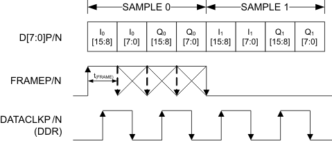 Figure 34. Byte-Wide Data Transmission Format
7.4.2 LVPECL Inputs
Figure 35 shows an equivalent circuit for the DAC input clock (DACCLKP/N) and the FIFO output strobe clock (OSTRP/N).
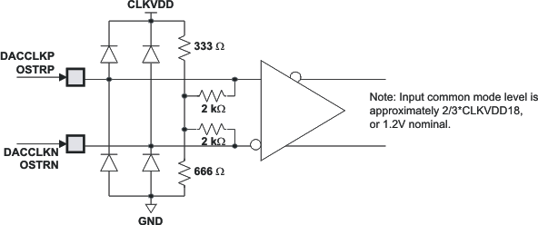 Figure 35. DACCLKP/N and OSTRP/N Equivalent Input Circuit
Figure 36 shows the preferred configuration for driving the CLKIN/CLKINC input clock with a differential ECL/PECL source.
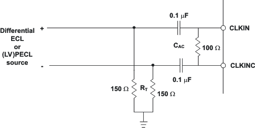 Figure 36. Preferred Clock Input Configuration With a Differential ECL/PECL Clock Source
7.4.3 LVDS Inputs
The D[7:0]P/N, DATACLKP/N and FRAMEP/N LVDS pairs have the input configuration shown in Figure 37. Figure 38 shows the typical input levels and common-move voltage used to drive these inputs.
![DAC3282 D[7:0]P/N, DATACLKP/N
and FRAMEP/N LVDS Input Configuration DAC3282 com_move_v_las646.gif](/ods/images/SLAS646C/com_move_v_las646.gif) Figure 37. D[7:0]P/N, DATACLKP/N and FRAMEP/N LVDS Input Configuration
Figure 37. D[7:0]P/N, DATACLKP/N and FRAMEP/N LVDS Input Configuration
![DAC3282 LVDS Data (D[7:0]P/N,
DATACLKP/N, FRAMEP/N Pairs) Input Levels DAC3282 lvds_data_las646.gif](/ods/images/SLAS646C/lvds_data_las646.gif) Figure 38. LVDS Data (D[7:0]P/N, DATACLKP/N, FRAMEP/N Pairs) Input Levels
Figure 38. LVDS Data (D[7:0]P/N, DATACLKP/N, FRAMEP/N Pairs) Input Levels
Table 5. Example LVDS Data Input Levels
| Applied Voltages | Resulting Differential Voltage | Resulting Common-Mode Voltage | Logical Bit Binary Equivalent | |
|---|---|---|---|---|
| VA | VB | VA,B | VCOM | |
| 1.4 V | 1.0 V | 400 mV | 1.2 V | 1 |
| 1.0 V | 1.4 V | –400 mV | 0 | |
| 1.2 V | 0.8 V | 400 mV | 1.0 V | 1 |
| 0.8 V | 1.2 V | –400 mV | 0 | |
7.4.4 CMOS Digital Inputs
Figure 39 shows a schematic of the equivalent CMOS digital inputs of the DAC3282. SDIO, SCLK and TXENABLE have pull-down resistors while SDENB and RESETB have pull-up resistors internal to the DAC3282. See the specification table for logic thresholds. The pull-up and pull-down circuitry is approximately equivalent to 100kΩ.
 Figure 39. CMOS/TTL Digital Equivalent Input
7.4.5 DAC Transfer Function
The CMOS DAC’s consist of a segmented array of NMOS current sinks, capable of sinking a full-scale output current up to 20 mA. Differential current switches direct the current to either one of the complementary output nodes IOUT1 or IOUT2. (DACA = IOUTA1 or IOUTA2 and DACB = IOUTB1 or IOUTB2.) Complementary output currents enable differential operation, thus canceling out common mode noise sources (digital feed-through, on-chip and PCB noise), dc offsets, even order distortion components, and increasing signal output power by a factor of two.
The full-scale output current is set using external resistor RBIAS in combination with an on-chip bandgap voltage reference source (+1.2V) and control amplifier. Current IBIAS through resistor RBIAS is mirrored internally to provide a maximum full-scale output current equal to 16 times IBIAS.
The relation between IOUT1 and IOUT2 can be expressed as:
IOUT1 = – IOUTFS – IOUT2
We will denote current flowing into a node as – current and current flowing out of a node as + current. Since the output stage is a current sink the current can only flow from AVDD into the IOUT1 and IOUT2 pins. The output current flow in each pin driving a resistive load can be expressed as:
IOUT1 = IOUTFS × (65535 – CODE) / 65536
IOUT2 = IOUTFS × CODE / 65536
where CODE is the decimal representation of the DAC data input word.
For the case where IOUT1 and IOUT2 drive resistor loads RL directly, this translates into single ended voltages at IOUT1 and IOUT2:
VOUT1 = AVDD – | IOUT1 | × RL
VOUT2 = AVDD – | IOUT2 | × RL
Assuming that the data is full scale (65536 in offset binary notation) and the RL is 25 Ω, the differential voltage between pins IOUT1 and IOUT2 can be expressed as:
VOUT1 = AVDD – | –0mA | × 25 Ω = 3.3 V
VOUT2 = AVDD – | –20mA | × 25 Ω = 2.8 V
VDIFF = VOUT1 – VOUT2 = 0.5V
Note that care should be taken not to exceed the compliance voltages at node IOUT1 and IOUT2, which would lead to increased signal distortion.
7.5 Programming
7.5.1 Serial Interface
The serial port of the DAC3282 is a flexible serial interface which communicates with industry standard microprocessors and microcontrollers. The interface provides read/write access to all registers used to define the operating modes of DAC3282. It is compatible with most synchronous transfer formats and can be configured as a 3 or 4 pin interface by sif4_ena in register CONFIG23. In both configurations, SCLK is the serial interface input clock and SDENB is serial interface enable. For 3 pin configuration, SDIO is a bidirectional pin for both data in and data out. For 4 pin configuration, SDIO is bidirectional and ALARM_SDO is data out only. Data is input into the device with the rising edge of SCLK. Data is output from the device on the falling edge of SCLK.
Each read/write operation is framed by signal SDENB (Serial Data Enable Bar) asserted low for 2 to 5 bytes, depending on the data length to be transferred (1–4 bytes). The first frame byte is the instruction cycle which identifies the following data transfer cycle as read or write, how many bytes to transfer, and what address to transfer the data. Table 6 indicates the function of each bit in the instruction cycle and is followed by a detailed description of each bit. Frame bytes 2 to 5 comprise the data transfer cycle.
Table 6. Instruction Byte of the Serial Interface
| MSB | LSB | |||||||
|---|---|---|---|---|---|---|---|---|
| Bit | 7 | 6 | 5 | 4 | 3 | 2 | 1 | 0 |
| Description | R/W | N1 | N0 | A4 | A3 | A2 | A1 | A0 |
| R/W | Identifies the following data transfer cycle as a read or write operation. A high indicates a read operation from DAC3282 and a low indicates a write operation to DAC3282. |
| [N1 : N0] | Identifies the number of data bytes to be transferred per Table 7. Data is transferred MSB first. |
Table 7. Number of Transferred Bytes Within One Communication Frame
| N1 | N0 | Description |
|---|---|---|
| 0 | 0 | Transfer 1 Byte |
| 0 | 1 | Transfer 2 Bytes |
| 1 | 0 | Transfer 3 Bytes |
| 1 | 1 | Transfer 4 Bytes |
| [A4 : A0] | Identifies the address of the register to be accessed during the read or write operation. For multi-byte transfers, this address is the starting address. Note that the address is written to the DAC3282 MSB first and counts down for each byte. |
Figure 40 shows the serial interface timing diagram for a DAC3282 write operation. SCLK is the serial interface clock input to DAC3282. Serial data enable SDENB is an active low input to DAC3282. SDIO is serial data in. Input data to DAC3282 is clocked on the rising edges of SCLK.
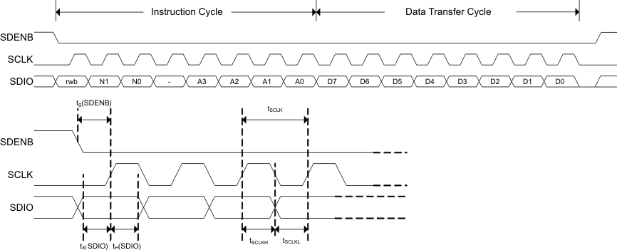 Figure 40. Serial Interface Write Timing Diagram
Figure 41 shows the serial interface timing diagram for a DAC3282 read operation. SCLK is the serial interface clock input to DAC3282. Serial data enable SDENB is an active low input to DAC3282. SDIO is serial data in during the instruction cycle. In 3 pin configuration, SDIO is data out from DAC3282 during the data transfer cycle(s), while ALARM_SDO is in a high-impedance state. In 4 pin configuration, both ALARM_SDO and SDIO are data out from DAC3282. At the end of the data transfer, ALARM_SDO will output low on the final falling edge of SCLK until the rising edge of SDENB when it will 3-state.
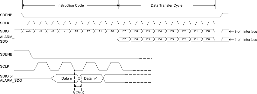 Figure 41. Serial Interface Read Timing Diagram
7.6 Register Maps
Table 8. Register Descriptions
7.6.1 CONFIG0 (address = 0x00) [reset = 0x70]
| 7 | 6 | 5 | 4 | 3 | 2 | 1 | 0 |
| qmc_offset_ena | fifoin_ena | fifo_reset_ena | multi_sync_ena | alarm_out_ena | alarm_pol | mixer_func | |
| R/W | R/W | R/W | R/W | R/W | R/W | R/W | R/W |
| LEGEND: R/W = Read/Write; R = Read only; -n = value after reset |
Table 9. CONFIG0 Field Descriptions
7.6.2 CONFIG1 (address = 0x01) [reset = 0x11]
| 7 | 6 | 5 | 4 | 3 | 2 | 1 | 0 |
| Unused | Unused | Unused | fir_ena | fir4_ena | iotest_ena | Unused | twos |
| R/W | R/W | R/W | R/W | R/W | R/W | R/W | R/W |
| LEGEND: R/W = Read/Write; R = Read only; -n = value after reset |
Table 10. CONFIG1 Field Descriptions
| Bit | Field | Type | Reset | Description |
|---|---|---|---|---|
| 7 | Unused | R/W | 0 | Reserved for factory use |
| 6 | Unused | R/W | 0 | Reserved for factory use. |
| 5 | Unused | R/W | 0 | Reserved for factory use |
| 4 | fir_ena | R/W | 1 | When asserted the chip does 2X interpolation of the data. |
| 3 | fir4_ena | R/W | 0 | When asserted, the zero-IF sinc correction filter is enabled. This filter cannot be used unless fir_ena is asserted. |
| 2 | iotest_ena | R/W | 0 | When asserted enables the data pattern checker operation. |
| 1 | Unused | R/W | 0 | Reserved for factory use. |
| 0 | twos | R/W | 1 | When asserted the inputs are expected to be in 2's complement format. When de-asserted the input format is expected to be offset-binary. |
7.6.3 CONFIG2 (address = 0x02) [reset = 0x00]
| 7 | 6 | 5 | 4 | 3 | 2 | 1 | 0 |
| Unused | Unused | Unused | Unused | output_delay | |||
| R/W | R/W | R/W | R/W | R/W | R/W | R/W | R/W |
| LEGEND: R/W = Read/Write; R = Read only; -n = value after reset |
Table 11. CONFIG2 Field Descriptions
| Bit | Field | Type | Reset | Description |
|---|---|---|---|---|
| 7 | Unused | R/W | 0 | Reserved for factory use. |
| 6 | Unused | R/W | 0 | Reserved for factory use. |
| 5 | Unused | R/W | 0 | Reserved for factory use. |
| 4 | Unused | R/W | 0 | Reserved for factory use. |
| 3:0 | output_delay | R/W | 0000 | Delays the output to the DACs from 0 to 15 DAC clock cycles. |
7.6.4 CONFIG3 (address = 0x03) [reset = 0x10]
| 7 | 6 | 5 | 4 | 3 | 2 | 1 | 0 |
| 64cnt_ena | Unused | Unused | fifo_offset | alarm_2away_ena | alarm_1away_ena | ||
| R/W | R/W | R/W | R/W | R/W | R/W | R/W | R/W |
| LEGEND: R/W = Read/Write; R = Read only; -n = value after reset |
Table 12. CONFIG3 Field Descriptions
7.6.5 CONFIG4 (address = 0x04) [reset = 0xFF]
| 7 | 6 | 5 | 4 | 3 | 2 | 1 | 0 |
| coarse_daca | coarse_dach | ||||||
| R/W | R/W | R/W | R/W | R/W | R/W | R/W | R/W |
| LEGEND: R/W = Read/Write; R = Read only; -n = value after reset |
Table 13. CONFIG4 Field Descriptions
| Bit | Field | Type | Reset | Description |
|---|---|---|---|---|
| 7:4 | coarse_daca | R/W | 1111 | Scales the DACA output current in 16 equal steps. |
 |
||||
| 3:0 | coarse_dach | R/W | 1111 | Scales the DACB output current in 16 equal steps. |
7.6.6 CONFIG5 (address = 0x05) READ ONLY
| 7 | 6 | 5 | 4 | 3 | 2 | 1 | 0 |
| tempdata | |||||||
| R | R | R | R | R | R | R | R |
| LEGEND: R/W = Read/Write; R = Read only; -n = value after reset |
Table 14. CONFIG5 Field Descriptions
| Bit | Field | Type | Reset | Description |
|---|---|---|---|---|
| 7:0 | tempdata | R | N/A | This is the output from the chip temperature sensor. The value of this register in two’s complement format represents the temperature in degrees Celsius. This register must be read with a minimum SCLK period of 1µs. (Read Only) |
7.6.7 CONFIG6 (address =0x06) [reset = 0x00]
| 7 | 6 | 5 | 4 | 3 | 2 | 1 | 0 |
| Unused | alarm_mask | ||||||
| R/W | R/W | R/W | R/W | R/W | R/W | R/W | R/W |
| LEGEND: R/W = Read/Write; R = Read only; -n = value after reset |
Table 15. CONFIG6 Field Descriptions
| Bit | Field | Type | Reset | Description | |
|---|---|---|---|---|---|
| 7 | Unused | R/W | 0 | Reserved for factory use. | |
| 6:0 | alarm_mask | R/W | 0000000 | These bits control the masking of the alarm outputs. This means that the ALARM_SDO pin will not be asserted if the appropriate bit is set. The alarm will still show up in the CONFIG7 bits. (0=not masked, 1= masked). | |
| alarm_mask | Masked Alarm | ||||
| 6 | alarm_from_zerochk | ||||
| 5 | alarm_fifo_collision | ||||
| 4 | reserved | ||||
| 3 | alarm_from_iotest | ||||
| 2 | not used (expansion) | ||||
| 1 | alarm_fifo_2away | ||||
| 0 | alarm_fifo_1away | ||||
7.6.8 CONFIG7 (address = 0x07) [reset = 0x00] (WRITE TO CLEAR)
| 7 | 6 | 5 | 4 | 3 | 2 | 1 | 0 |
| Unused | alarm_from_ zerochk |
alarm_fifo_ collision |
Reserved | alarm_from_ iotest |
Unused | alarm_fifo_ 2away |
alarm_fifo_ 1away |
| W | W | W | W | W | W | W | W |
| LEGEND: R/W = Read/Write; R = Read only; -n = value after reset |
Table 16. CONFIG7 Field Descriptions
7.6.9 CONFIG8 (address = 0x08) [reset = 0x00] (WRITE TO CLEAR)
| 7 | 6 | 5 | 4 | 3 | 2 | 1 | 0 |
| iotest_results | |||||||
| R/W | R/W | R/W | R/W | R/W | R/W | R/W | R/W |
| LEGEND: R/W = Read/Write; R = Read only; -n = value after reset |
Table 17. CONFIG8 Field Descriptions
| Bit | Field | Type | Reset | Description |
|---|---|---|---|---|
| 7:0 | iotest_results | R/W | 0x00 | The values of these bits tell which bit in the byte-wide LVDS bus failed during the pattern checker test. |
7.6.10 CONFIG9 (address = 0x09) [reset = 0x7A]
| 7 | 6 | 5 | 4 | 3 | 2 | 1 | 0 |
| iotest_pattern0 | |||||||
| R/W | R/W | R/W | R/W | R/W | R/W | R/W | R/W |
| LEGEND: R/W = Read/Write; R = Read only; -n = value after reset |
Table 18. CONFIG9 Field Descriptions
| Bit | Field | Type | Reset | Description |
|---|---|---|---|---|
| 7:0 | iotest_pattern0 | R/W | 0x7A | This is dataword0 in the IO test pattern. It is used with the seven other words to test the input data. |
7.6.11 CONFIG10 (address = 0x0A) [reset = 0xB6]
| 7 | 6 | 5 | 4 | 3 | 2 | 1 | 0 |
| iotest_pattern1 | |||||||
| R/W | R/W | R/W | R/W | R/W | R/W | R/W | R/W |
| LEGEND: R/W = Read/Write; R = Read only; -n = value after reset |
Table 19. CONFIG10 Field Descriptions
| Bit | Field | Type | Reset | Description |
|---|---|---|---|---|
| 7:0 | iotest_pattern1 | R/W | 0xB6 | This is dataword1 in the IO test pattern. It is used with the seven other words to test the input data. |
7.6.12 CONFIG11 (address = 0x0B) [reset = 0xEA]
| 7 | 6 | 5 | 4 | 3 | 2 | 1 | 0 |
| iotest_pattern2 | |||||||
| R/W | R/W | R/W | R/W | R/W | R/W | R/W | R/W |
| LEGEND: R/W = Read/Write; R = Read only; -n = value after reset |
Table 20. CONFIG11 Field Descriptions
| Bit | Field | Type | Reset | Description |
|---|---|---|---|---|
| 7:0 | iotest_pattern2 | R/W | 0xEA | This is dataword2 in the IO test pattern. It is used with the seven other words to test the input data. |
7.6.13 CONFIG12 (address =0x0C) [reset = 0x45]
| 7 | 6 | 5 | 4 | 3 | 2 | 1 | 0 |
| iotest_pattern3 | |||||||
| R/W | R/W | R/W | R/W | R/W | R/W | R/W | R/W |
| LEGEND: R/W = Read/Write; R = Read only; -n = value after reset |
Table 21. CONFIG12 Field Descriptions
| Bit | Field | Type | Reset | Description |
|---|---|---|---|---|
| 7:0 | iotest_pattern3 | R/W | 0x45 | This is dataword3 in the IO test pattern. It is used with the seven other words to test the input data. |
7.6.14 CONFIG13 (address =0x0D) [reset = 0x1A]
| 7 | 6 | 5 | 4 | 3 | 2 | 1 | 0 |
| iotest_pattern4 | |||||||
| R/W | R/W | R/W | R/W | R/W | R/W | R/W | R/W |
| LEGEND: R/W = Read/Write; R = Read only; -n = value after reset |
Table 22. CONFIG13 Field Descriptions
| Bit | Field | Type | Reset | Description |
|---|---|---|---|---|
| 7:0 | iotest_pattern4 | R/W | 0x1A | This is dataword4 in the IO test pattern. It is used with the seven other words to test the input data. |
7.6.15 CONFIG14 Register Name (address = 0x0E) [reset = 0x16]
| 7 | 6 | 5 | 4 | 3 | 2 | 1 | 0 |
| iotest_pattern5 | |||||||
| R/W | R/W | R/W | R/W | R/W | R/W | R/W | R/W |
| LEGEND: R/W = Read/Write; R = Read only; -n = value after reset |
Table 23. CONFIG14 Field Descriptions
| Bit | Field | Type | Reset | Description |
|---|---|---|---|---|
| 7:0 | iotest_pattern5 | R/W | 0x16 | This is dataword5 in the IO test pattern. It is used with the seven other words to test the input data. |
7.6.16 CONFIG15 Register Name (address = 0x0F) [reset = 0xAA]
| 7 | 6 | 5 | 4 | 3 | 2 | 1 | 0 |
| iotest_pattern6 | |||||||
| R/W | R/W | R/W | R/W | R/W | R/W | R/W | R/W |
| LEGEND: R/W = Read/Write; R = Read only; -n = value after reset |
Table 24. CONFIG15 Field Descriptions
| Bit | Field | Type | Reset | Description |
|---|---|---|---|---|
| 7:0 | iotest_pattern6 | R/W | 0xAA | This is dataword6 in the IO test pattern. It is used with the seven other words to test the input data. |
7.6.17 CONFIG16 (address = 0x10) [reset = 0xC6]
| 7 | 6 | 5 | 4 | 3 | 2 | 1 | 0 |
| iotest_pattern7 | |||||||
| R/W | R/W | R/W | R/W | R/W | R/W | R/W | R/W |
| LEGEND: R/W = Read/Write; R = Read only; -n = value after reset |
Table 25. CONFIG16 Field Descriptions
| Bit | Field | Type | Reset | Description |
|---|---|---|---|---|
| 7:0 | iotest_pattern7 | R/W | 0xC6 | This is dataword7 in the IO test pattern. It is used with the seven other words to test the input data. |
7.6.18 CONFIG17 (address = 0x11) [reset = 0x00]
| 7 | 6 | 5 | 4 | 3 | 2 | 1 | 0 |
| Reserved | Reserved | Reserved | Reserved | Reserved | Reserved | Reserved | Reserved |
| R/W | R/W | R/W | R/W | R/W | R/W | R/W | R/W |
| LEGEND: R/W = Read/Write; R = Read only; -n = value after reset |
Table 26. CONFIG17 Field Descriptions
| Bit | Field | Type | Reset | Description |
|---|---|---|---|---|
| 7:6 | Reserved | R/W | 00 | Reserved for factory use. |
| 5 | Reserved | R/W | 0 | Reserved for factory use. |
| 4 | Reserved | R/W | 0 | Reserved for factory use. |
| 3:0 | Reserved | R/W | 0000 | Reserved for factory use. |
7.6.19 CONFIG18 (address = 0x12) [reset = 0x02]
| 7 | 6 | 5 | 4 | 3 | 2 | 1 | 0 |
| Reserved | daca_complement | dacb_complement | clkdiv_sync_ena | Unused | |||
| R/W | R/W | R/W | R/W | R/W | R/W | R/W | R/W |
| LEGEND: R/W = Read/Write; R = Read only; -n = value after reset |
Table 27. CONFIG18 Field Descriptions
7.6.20 CONFIG19 (address = 0x13) [reset = 0x00]
| 7 | 6 | 5 | 4 | 3 | 2 | 1 | 0 |
| bequalsa | aequalsb | Reserved | Unused | Unused | Unused | multi_sync_sel | rev |
| R/W | R/W | R/W | R/W | R/W | R/W | R/W | R/W |
| LEGEND: R/W = Read/Write; R = Read only; -n = value after reset |
Table 28. CONFIG19 Field Descriptions
| Bit | Field | Type | Reset | Description | |
|---|---|---|---|---|---|
| 7 | bequalsa | R/W | 0 | When asserted the DACA data is driven onto DACB. | |
| 6 | aequalsb | R/W | 0 | When asserted the DACB data is driven onto DACA. | |
| 5 | Reserved | R/W | 0 | Reserved for factory use. | |
| 4 | Unused | R/W | 0 | Reserved for factory use. | |
| 3 | Unused | R/W | 0 | Reserved for factory use. | |
| 2 | Unused | R/W | 0 | Reserved for factory use. | |
| 1 | multi_sync_sel | R/W | 0 | Selects the signal source for multiple device and clock divider synchronization. | |
| multi_sync_sel | Sync Source | ||||
| 0 | OSTR | ||||
| 1 | FRAME through FIFO handoff | ||||
| 0 | rev | R/W | 0 | Reverse the input bits for the data word. MSB becomes LSB. | |
7.6.21 CONFIG20 (address = 0x14) [reset = 0x00] (CAUSES AUTOSYNC)
| 7 | 6 | 5 | 4 | 3 | 2 | 1 | 0 |
| qmc_offseta | |||||||
| R/W | R/W | R/W | R/W | R/W | R/W | R/W | R/W |
| LEGEND: R/W = Read/Write; R = Read only; -n = value after reset |
Table 29. CONFIG20 Field Descriptions
| Bit | Field | Type | Reset | Description |
|---|---|---|---|---|
| 7:0 | qmc_offseta | R/W | 0x00 | Lower 8 bits of the DAC A offset correction. The offset is measured in DAC LSBs. Writing this register causes an autosync to be generated. This loads the values of all four qmc_offset registers (CONFIG20-CONFIG23) into the offset block at the same time. When updating the offset values CONFIG20 should be written last. Programming any of the other three registers will not affect the offset setting. |
7.6.22 CONFIG21 (address = 0x15) [reset = 0x00]
| 7 | 6 | 5 | 4 | 3 | 2 | 1 | 0 |
| qmc_offsetb | |||||||
| R/W | R/W | R/W | R/W | R/W | R/W | R/W | R/W |
| LEGEND: R/W = Read/Write; R = Read only; -n = value after reset |
Table 30. CONFIG21 Field Descriptions
| Bit | Field | Type | Reset | Description |
|---|---|---|---|---|
| 7:0 | qmc_offsetb | R/W | 0x00 | Lower 8 bits of the DAC B offset correction. The offset is measured in DAC LSBs. |
7.6.23 CONFIG22 (address = 0x16) [reset = 0x00]
| 7 | 6 | 5 | 4 | 3 | 2 | 1 | 0 |
| qmc_offseta | Unused | Unused | Unused | ||||
| R/W | R/W | R/W | R/W | R/W | R/W | R/W | R/W |
| LEGEND: R/W = Read/Write; R = Read only; -n = value after reset |
Table 31. CONFIG22 Field Descriptions
| Bit | Field | Type | Reset | Description |
|---|---|---|---|---|
| 7:3 | qmc_offseta | R/W | 00000 | Upper 5 bits of the DAC A offset correction. |
| 2 | Unused | R/W | 0 | Reserved for factory use. |
| 1 | Unused | R/W | 0 | Reserved for factory use. |
| 0 | Unused | R/W | 0 | Reserved for factory use. |
7.6.24 CONFIG23 (address = 0x17) [reset = 0x00]
| 7 | 6 | 5 | 4 | 3 | 2 | 1 | 0 |
| qmc_offsetb(12:8) | sif4_ena | clkpath_sleep_a | clkpath_sleep_b | ||||
| R/W | R/W | R/W | R/W | R/W | R/W | R/W | R/W |
| LEGEND: R/W = Read/Write; R = Read only; -n = value after reset |
Table 32. CONFIG23 Field Descriptions
| Bit | Field | Type | Reset | Description |
|---|---|---|---|---|
| 7:3 | qmc_offsetb(12:8) | R/W | 00000 | Upper 5 bits of the DAC B offset correction. |
| 2 | sif4_ena | R/W | 0 | When asserted the SIF interface becomes a 4 pin interface. The ALARM_SDO pin is turned into a dedicated output for the reading of data. |
| 1 | clkpath_sleep_a | R/W | 0 | When asserted puts the clock path through DAC A to sleep. This is useful for sleeping individual DACs. Even if the DAC is asleep the clock needs to pass through it for the logic to work. However, if the chip is being put into a power down mode, then all parts of the DAC can be turned off. |
| 0 | clkpath_sleep_b | R/W | 0 | When asserted puts the clock path through DAC B to sleep. |
7.6.25 CONFIG24 (address = 0x18) [reset = 0x83]
| 7 | 6 | 5 | 4 | 3 | 2 | 1 | 0 |
| tsense_ena | clkrecv_sleep | Unused | Reserved | sleepb | sleepa | Reserved | Reserved |
| R/W | R/W | R/W | R/W | R/W | R/W | R/W | R/W |
| LEGEND: R/W = Read/Write; R = Read only; -n = value after reset |
Table 33. CONFIG24 Field Descriptions
| Bit | Field | Type | Reset | Description |
|---|---|---|---|---|
| 7 | tsense_ena | R/W | 1 | Turns on the temperature sensor when asserted. |
| 6 | clkrecv_sleep | R/W | 0 | When asserted the clock input receiver gets put into sleep mode. This also affects the OSTR receiver. |
| 5 | Unused | R/W | 0 | Reserved for factory use. |
| 4 | Reserved | R/W | 0 | Reserved for factory use. |
| 3 | sleepb | R/W | 0 | When asserted DACB is put into sleep mode. |
| 2 | sleepa | R/W | 0 | When asserted DACA is put into sleep mode. |
| 1 | Reserved | R/W | 1 | Reserved for factory use. |
| 0 | Reserved | R/W | 1 | Reserved for factory use. |
7.6.26 CONFIG25 (address = 0x19) [reset = 0x00]
| 7 | 6 | 5 | 4 | 3 | 2 | 1 | 0 |
| Reserved | extref_ena | Reserved | Reserved | ||||
| R/W | R/W | R/W | R/W | R/W | R/W | R/W | R/W |
| LEGEND: R/W = Read/Write; R = Read only; -n = value after reset |
Table 34. CONFIG25 Field Descriptions
| Bit | Field | Type | Reset | Description |
|---|---|---|---|---|
| 7:3 | Reserved | R/W | 00000 | Reserved for factory use. |
| 2 | extref_ena | R/W | 0 | Allows the device to use an external reference or the internal reference. (0=internal, 1=external) |
| 1 | Reserved | R/W | 0 | Reserved for factory use. |
| 0 | Reserved | R/W | 0 | Reserved for factory use. |
7.6.27 CONFIG26 (address = 0x1A) [reset = 0x00]
| 7 | 6 | 5 | 4 | 3 | 2 | 1 | 0 |
| Reserved | Reserved | Reserved | Reserved | Unused | Reserved | ||
| R/W | R/W | R/W | R/W | R/W | R/W | R/W | R/W |
| LEGEND: R/W = Read/Write; R = Read only; -n = value after reset |
Table 35. CONFIG26 Field Descriptions
| Bit | Field | Type | Reset | Description |
|---|---|---|---|---|
| 7 | Reserved | R/W | 0 | Reserved for factory use. |
| 6 | Reserved | R/W | 0 | Reserved for factory use. |
| 5 | Reserved | R/W | 0 | Reserved for factory use. |
| 5 | Reserved | R/W | 0 | Reserved for factory use. |
| 3 | Unused | R/W | 0 | Reserved for factory use. |
| 2:0 | Reserved | R/W | 000 | Reserved for factory use. |
7.6.28 CONFIG27 (address =0x1B) [reset = 0x00]
| 7 | 6 | 5 | 4 | 3 | 2 | 1 | 0 |
| Reserved | |||||||
| R/W | R/W | R/W | R/W | R/W | R/W | R/W | R/W |
| LEGEND: R/W = Read/Write; R = Read only; -n = value after reset |
Table 36. CONFIG27 Field Descriptions
| Bit | Field | Type | Reset | Description |
|---|---|---|---|---|
| 7:0 | Reserved | R/W | 0x00 | Reserved for factory use. |
7.6.29 CONFIG28 (address = 0x1C) [reset = 0x00]
| 7 | 6 | 5 | 4 | 3 | 2 | 1 | 0 |
| Reserved | |||||||
| R/W | R/W | R/W | R/W | R/W | R/W | R/W | R/W |
| LEGEND: R/W = Read/Write; R = Read only; -n = value after reset |
Table 37. CONFIG28 Field Descriptions
| Bit | Field | Type | Reset | Description |
|---|---|---|---|---|
| 7:0 | Reserved | R/W | 0x00 | Reserved for factory use. |
7.6.30 CONFIG29 (address = 0x1D) [reset = 0x00]
| 7 | 6 | 5 | 4 | 3 | 2 | 1 | 0 |
| Reserved | |||||||
| R/W | R/W | R/W | R/W | R/W | R/W | R/W | R/W |
| LEGEND: R/W = Read/Write; R = Read only; -n = value after reset |
Table 38. CONFIG29 Field Descriptions
| Bit | Field | Type | Reset | Description |
|---|---|---|---|---|
| 7:0 | Reserved | R/W | 0x00 | Reserved for factory use. |
7.6.31 CONFIG30 (address = 0x1E) [reset = 0x00]
| 7 | 6 | 5 | 4 | 3 | 2 | 1 | 0 |
| Reserved | |||||||
| R/W | R/W | R/W | R/W | R/W | R/W | R/W | R/W |
| LEGEND: R/W = Read/Write; R = Read only; -n = value after reset |
Table 39. CONFIG30 Field Descriptions
| Bit | Field | Type | Reset | Description |
|---|---|---|---|---|
| 7:0 | Reserved | R/W | 0x00 | Reserved for factory use. |
7.6.32 VERSION31 (address = 0x1F) [reset = 0x43] (READ ONLY)
| 7 | 6 | 5 | 4 | 3 | 2 | 1 | 0 |
| deviceid | version | ||||||
| R | R | R | R | R | R | R | R |
| LEGEND: R/W = Read/Write; R = Read only; -n = value after reset |
