JAJSSV2G March 2011 – January 2024 DAC3482
PRODUCTION DATA
- 1
- 1 特長
- 2 アプリケーション
- 3 概要
- 4 Pin Configuration and Functions
-
5 Specifications
- 5.1 Absolute Maximum Ratings
- 5.2 ESD Ratings
- 5.3 Recommended Operating Conditions
- 5.4 Thermal Information
- 5.5 Electrical Characteristics – DC Specifications
- 5.6 Electrical Characteristics – Digital Specifications
- 5.7 Electrical Characteristics – AC Specifications
- 5.8 Electrical Characteristics - Phase-Locked Loop Specifications
- 5.9 Timing Requirements - Digital Specifications
- 5.10 Switching Characteristics – AC Specifications
- 5.11 Typical Characteristics
-
6 Detailed Description
- 6.1 Overview
- 6.2 Functional Block Diagram
- 6.3
Feature Description
- 6.3.1 Serial Interface
- 6.3.2 Data Interface
- 6.3.3 Input FIFO
- 6.3.4 FIFO Modes of Operation
- 6.3.5 Clocking Modes
- 6.3.6 FIR Filters
- 6.3.7 Complex Signal Mixer
- 6.3.8 Quadrature Modulation Correction (QMC)
- 6.3.9 Temperature Sensor
- 6.3.10 Data Pattern Checker
- 6.3.11 Parity Check Test
- 6.3.12 DAC3482 Alarm Monitoring
- 6.3.13 LVPECL Inputs
- 6.3.14 LVDS Inputs
- 6.3.15 Unused LVDS Port Termination
- 6.3.16 CMOS Digital Inputs
- 6.3.17 Reference Operation
- 6.3.18 DAC Transfer Function
- 6.3.19 Analog Current Outputs
- 6.4 Device Functional Modes
- 6.5 Programming
- 6.6
Register Map
- 6.6.1
Register Descriptions
- 6.6.1.1 Register Name: config0 – Address: 0x00, Default: 0x049C
- 6.6.1.2 Register Name: config1 – Address: 0x01, Default: 0x050E
- 6.6.1.3 Register Name: config2 – Address: 0x02, Default: 0x7000
- 6.6.1.4 Register Name: config3 – Address: 0x03, Default: 0xF000
- 6.6.1.5 Register Name: config4 – Address: 0x04, Default: No RESET Value (WRITE TO CLEAR)
- 6.6.1.6 Register Name: config5 – Address: 0x05, Default: Setup and Power-Up Conditions Dependent (WRITE TO CLEAR)
- 6.6.1.7 Register Name: config6 – Address: 0x06, Default: No RESET Value (READ ONLY)
- 6.6.1.8 Register Name: config7 – Address: 0x07, Default: 0xFFFF
- 6.6.1.9 Register Name: config8 – Address: 0x08, Default: 0x0000 (CAUSES AUTO-SYNC)
- 6.6.1.10 Register Name: config9 – Address: 0x09, Default: 0x8000
- 6.6.1.11 Register Name: config10 – Address: 0x0A, Default: 0x0000
- 6.6.1.12 Register Name: config11 – Address: 0x0B, Default: 0x0000
- 6.6.1.13 Register Name: config12 – Address: 0x0C, Default: 0x0400
- 6.6.1.14 Register Name: config13 – Address: 0x0D, Default: 0x0400
- 6.6.1.15 Register Name: config14 – Address: 0x0E, Default: 0x0400
- 6.6.1.16 Register Name: config15 – Address: 0x0F, Default: 0x0400
- 6.6.1.17 Register Name: config16 – Address: 0x10, Default: 0x0000 (CAUSES AUTO-SYNC)
- 6.6.1.18 Register Name: config17 – Address: 0x11, Default: 0x0000
- 6.6.1.19 Register Name: config18 – Address: 0x12, Default: 0x0000 (CAUSES AUTO-SYNC)
- 6.6.1.20 Register Name: config19 – Address: 0x13, Default: 0x0000
- 6.6.1.21 Register Name: config20 – Address: 0x14, Default: 0x0000
- 6.6.1.22 Register Name: config21 – Address: 0x15, Default: 0x0000
- 6.6.1.23 Register name: config22 – Address: 0x16, Default: 0x0000
- 6.6.1.24 Register Name: config23 – Address: 0x17, Default: 0x0000
- 6.6.1.25 Register Name: config24 – Address: 0x18, Default: NA
- 6.6.1.26 Register Name: config25 – Address: 0x19, Default: 0x0440
- 6.6.1.27 Register Name: config26 – Address: 0x1A, Default: 0x0020
- 6.6.1.28 Register Name: config27 – Address: 0x1B, Default: 0x0000
- 6.6.1.29 Register Name: config28 – Address: 0x1C, Default: 0x0000
- 6.6.1.30 Register Name: config29 – Address: 0x1D, Default: 0x0000
- 6.6.1.31 Register Name: config30 – Address: 0x1E, Default: 0x1111
- 6.6.1.32 Register Name: config31 – Address: 0x1F, Default: 0x1140
- 6.6.1.33 Register Name: config32 – Address: 0x20, Default: 0x2400
- 6.6.1.34 Register Name: config33 – Address: 0x21, Default: 0x0000
- 6.6.1.35 Register Name: config34 – Address: 0x22, Default: 0x1B1B
- 6.6.1.36 Register Name: config35 – Address: 0x23, Default: 0xFFFF
- 6.6.1.37 Register Name: config36 – Address: 0x24, Default: 0x0000
- 6.6.1.38 Register Name: config37 – Address: 0x25, Default: 0x7A7A
- 6.6.1.39 Register Name: config38 – Address: 0x26, Default: 0xB6B6
- 6.6.1.40 Register Name: config39 – Address: 0x27, Default: 0xEAEA
- 6.6.1.41 Register Name: config40 – Address: 0x28, Default: 0x4545
- 6.6.1.42 Register Name: config41 – Address: 0x29, Default: 0x1A1A
- 6.6.1.43 Register Name: config42 – Address: 0x2A, Default: 0x1616
- 6.6.1.44 Register Name: config43 – Address: 0x2B, Default: 0xAAAA
- 6.6.1.45 Register Name: config44 – Address: 0x2C, Default: 0xC6C6
- 6.6.1.46 Register Name: config45 – Address: 0x2D, Default: 0x0004
- 6.6.1.47 Register Name: config46 – Address: 0x2E, Default: 0x0000
- 6.6.1.48 Register Name: config47 – Address: 0x2F, Default: 0x0000
- 6.6.1.49 Register Name: config48 – Address: 0x30, Default: 0x0000
- 6.6.1.50 Register Name: version– Address: 0x7F, Default: 0x540C (READ ONLY)
- 6.6.1
Register Descriptions
- 7 Application and Implementation
- 8 Device and Documentation Support
- 9 Revision History
- 10Mechanical, Packaging, and Orderable Information
パッケージ・オプション
メカニカル・データ(パッケージ|ピン)
サーマルパッド・メカニカル・データ
- RKD|88
発注情報
6.4.1.1 Multi-Device Synchronization: PLL Bypassed with Dual Sync Sources Mode
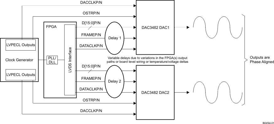
For single or multi-device synchronization it is important that delay differences in the data are absorbed by the device so that latency through the device remains the same. Furthermore, the outputs from each DAC are phase aligned it is necessary that data is read from the FIFO of each device simultaneously. In the DAC3482 this is accomplished by operating the multiple devices in Dual Sync Sources mode. In this mode, the additional OSTR signal is required by each DAC3482 to be synchronized.
Data into the device is input as LVDS signals from one or multiple baseband ASICs or FPGAs. Data into the multiple DAC devices can experience different delays due to variations in the digital source output paths or board level wiring. These different delays can be effectively absorbed by the DAC3482 FIFO so that all outputs are phase aligned correctly.
 Figure 6-39 Synchronization System in Dual Sync Sources Mode with PLL Bypassed
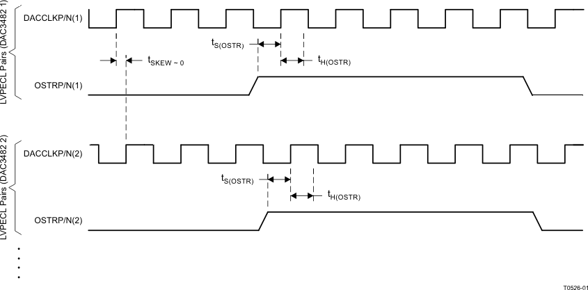
For correct operation both OSTR and DACCLK must be generated from the same clock domain. The OSTR signal is sampled by DACCLK and must satisfy the timing requirements in Section 5.9. If the clock generator does not have the ability to delay the DACCLK to meet the OSTR timing requirement, the polarity of the DACCLK outputs can be swapped with respect to the OSTR ones to create 180 degree phase delay of the DACCLK. This may help establish proper setup and hold time requirement of the OSTR signal.
Careful board layout planning must be done so the DACCLK and OSTR signals are distributed from device to device with the lowest skew possible as this will affect the synchronization process. To minimize the skew across devices, it is recommended to use the same clock distribution device to provide the DACCLK and OSTR signals to all the DAC devices in the system.
 Figure 6-40 Timing Diagram for LVPECL Synchronization Signals
The following steps are required to make sure the devices are fully synchronized. The procedure assumes all the DAC3482 devices have a DACCLK and OSTR signal and must be carried out on each device.
- Start-up the device as described in the power-up sequence. Set the DAC3482 in Dual Sync Sources mode and select OSTR as the clock divider sync source (clkdiv_sync_sel in register config32).
- Sync the clock divider and FIFO pointers.
- Verify there are no FIFO alarms either through register config5 or through the ALARM pin.
- Disable clock divider sync by setting clkdiv_sync_ena to “0” in register config0.
After these steps all the DAC3482 outputs will be synchronized.