JAJSLQ6A April 2021 – December 2021 DAC53004 , DAC63004
PRODUCTION DATA
- 1 特長
- 2 アプリケーション
- 3 概要
- 4 Revision History
- 5 Pin Configuration and Functions
-
6 Specifications
- 6.1 Absolute Maximum Ratings
- 6.2 ESD Ratings
- 6.3 Recommended Operating Conditions
- 6.4 Thermal Information
- 6.5 Electrical Characteristics: Voltage Output
- 6.6 Electrical Characteristics: Current Output
- 6.7 Electrical Characteristics: Comparator Mode
- 6.8 Electrical Characteristics: General
- 6.9 Timing Requirements: I2C Standard Mode
- 6.10 Timing Requirements: I2C Fast Mode
- 6.11 Timing Requirements: I2C Fast Mode Plus
- 6.12 Timing Requirements: SPI Write Operation
- 6.13 Timing Requirements: SPI Read and Daisy Chain Operation (FSDO = 0)
- 6.14 Timing Requirements: SPI Read and Daisy Chain Operation (FSDO = 1)
- 6.15 Timing Requirements: GPIO
- 6.16 Timing Diagrams
- 6.17 Typical Characteristics: Voltage Output
- 6.18 Typical Characteristics: Current Output
- 6.19 Typical Characteristics: Comparator
- 6.20 Typical Characteristics: General
-
7 Detailed Description
- 7.1 Overview
- 7.2 Functional Block Diagram
- 7.3 Feature Description
- 7.4 Device Functional Modes
- 7.5 Programming
- 7.6
Register Map
- 7.6.1 NOP Register (address = 00h) [reset = 0000h]
- 7.6.2 DAC-X-MARGIN-HIGH Register (address = 01h, 07h, 0Dh, 13h) [reset = 0000h]
- 7.6.3 DAC-X-MARGIN-LOW Register (address = 02h, 08h, 0Eh, 14h) [reset = 0000h]
- 7.6.4 DAC-X-VOUT-CMP-CONFIG Register (address = 03h, 09h, 0Fh, 15h) [reset = 0000h]
- 7.6.5 DAC-X-IOUT-MISC-CONFIG Register (address = 04h, 0Ah, 10h, 16h) [reset = 0000h]
- 7.6.6 DAC-X-CMP-MODE-CONFIG Register (address = 05h, 0Bh, 11h, 17h) [reset = 0000h]
- 7.6.7 DAC-X-FUNC-CONFIG Register (address = 06h, 0Ch, 12h, 18h) [reset = 0000h]
- 7.6.8 DAC-X-DATA Register (address = 19h, 1Ah, 1Bh, 1Ch) [reset = 0000h]
- 7.6.9 COMMON-CONFIG Register (address = 1Fh) [reset = 0FFFh]
- 7.6.10 COMMON-TRIGGER Register (address = 20h) [reset = 0000h]
- 7.6.11 COMMON-DAC-TRIG Register (address = 21h) [reset = 0000h]
- 7.6.12 GENERAL-STATUS Register (address = 22h) [reset = 00h, DEVICE-ID, VERSION-ID]
- 7.6.13 CMP-STATUS Register (address = 23h) [reset = 0000h]
- 7.6.14 GPIO-CONFIG Register (address = 24h) [reset = 0000h]
- 7.6.15 DEVICE-MODE-CONFIG Register (address = 25h) [reset = 0000h]
- 7.6.16 INTERFACE-CONFIG Register (address = 26h) [reset = 0000h]
- 7.6.17 SRAM-CONFIG Register (address = 2Bh) [reset = 0000h]
- 7.6.18 SRAM-DATA Register (address = 2Ch) [reset = 0000h]
- 7.6.19 DAC-X-DATA-8BIT Register (address = 40h, 41h, 42h, 43h) [reset = 0000h]
- 7.6.20 BRDCAST-DATA Register (address = 50h) [reset = 0000h]
- 7.6.21 PMBUS-PAGE Register [reset = 0300h]
- 7.6.22 PMBUS-OP-CMD-X Register [reset = 0000h]
- 7.6.23 PMBUS-CML Register [reset = 0000h]
- 7.6.24 PMBUS-VERSION Register [reset = 2200h]
- 8 Application and Implementation
- 9 Power Supply Recommendations
- 10Layout
- 11Device and Documentation Support
- 12Mechanical, Packaging, and Orderable Information
パッケージ・オプション
メカニカル・データ(パッケージ|ピン)
- RTE|16
サーマルパッド・メカニカル・データ
- RTE|16
発注情報
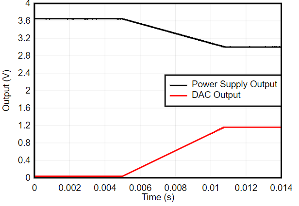
8.2.3 Application Curves
 Figure 8-2 Power-Supply Margin High
 Figure 8-3 Power-Supply Margin Low.