SBAS334D November 2004 – July 2016 DAC5675A
PRODUCTION DATA.
- 1 Features
- 2 Applications
- 3 Description
- 4 Revision History
- 5 Description Continued
- 6 Pin Configuration and Functions
- 7 Specifications
- 8 Detailed Description
- 9 Application and Implementation
- 10Power Supply Recommendations
- 11Layout
- 12Device and Documentation Support
- 13Mechanical, Packaging, and Orderable Information
パッケージ・オプション
メカニカル・データ(パッケージ|ピン)
- PHP|48
サーマルパッド・メカニカル・データ
- PHP|48
発注情報
11 Layout
11.1 Layout Guidelines
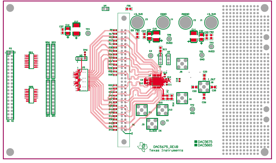
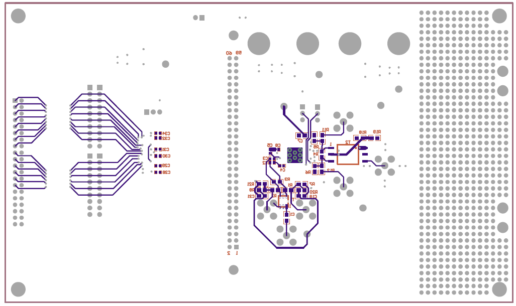
The DAC5675 EVM layout should be used as a reference for the layout to obtain the best performance. A sample layout is shown in Figure 27. Some important layout recommendations are:
- Use a single ground plane. Keep the digital and analog signals on distinct separate sections of the board. This may be virtually divided down the middle of the device package when doing placement and layout.
- Keep the analog outputs as far away from the switching clocks and digital signals as possible. This will keep coupling from the digital circuits to the analog outputs to a minimum.
- Decoupling caps should be kept close to the power pins of the device.
11.2 Layout Example
 Figure 27. Top Layer of DAC5675A EVM Layout
 Figure 28. Bottom Layer of DAC5675A EVM Layout