SLAS719E August   2010  – June 2015 DAC7562 , DAC7563 , DAC8162 , DAC8163 , DAC8562 , DAC8563

PRODUCTION DATA.  

  1. Features
  2. Applications
  3. Description
  4. Revision History
  5. Device Comparison Table
  6. Pin Configuration and Functions
  7. Specifications
    1. 7.1 Absolute Maximum Ratings
    2. 7.2 ESD Ratings
    3. 7.3 Recommended Operating Conditions
    4. 7.4 Thermal Information
    5. 7.5 Electrical Characteristics
    6. 7.6 Timing Requirements
    7. 7.7 Typical Characteristics
      1. 7.7.1 Typical Characteristics: Internal Reference
      2. 7.7.2 Typical Characteristics: DAC at AVDD = 5.5 V
      3. 7.7.3 Typical Characteristics: DAC at AVDD = 3.6 V
      4. 7.7.4 Typical Characteristics: DAC at AVDD = 2.7 V
  8. Detailed Description
    1. 8.1 Overview
    2. 8.2 Functional Block Diagram
    3. 8.3 Feature Description
      1. 8.3.1 Digital-to-Analog Converter (DAC)
        1. 8.3.1.1 Resistor String
        2. 8.3.1.2 Output Amplifier
      2. 8.3.2 Internal Reference
      3. 8.3.3 Power-On Reset
        1. 8.3.3.1 Power-On Reset to Zero-Scale
        2. 8.3.3.2 Power-On Reset to Mid-Scale
        3. 8.3.3.3 Power-On Reset (POR) Levels
    4. 8.4 Device Functional Modes
      1. 8.4.1 Power-Down Modes
        1. 8.4.1.1 DAC Power-Down Commands
      2. 8.4.2 Gain Function
      3. 8.4.3 Software Reset Function
      4. 8.4.4 Internal Reference Enable Register
        1. 8.4.4.1 Enabling Internal Reference
        2. 8.4.4.2 Disabling Internal Reference
      5. 8.4.5 CLR Functionality
      6. 8.4.6 LDAC Functionality
    5. 8.5 Programming
      1. 8.5.1 SYNC Interrupt
      2. 8.5.2 DAC Register Configuration
  9. Application and Implementation
    1. 9.1 Application Information
      1. 9.1.1 DAC Internal Reference
        1. 9.1.1.1 Supply Voltage
        2. 9.1.1.2 Temperature Drift
        3. 9.1.1.3 Noise Performance
        4. 9.1.1.4 Load Regulation
          1. 9.1.1.4.1 Long-Term Stability
        5. 9.1.1.5 Thermal Hysteresis
      2. 9.1.2 DAC Noise Performance
    2. 9.2 Typical Applications
      1. 9.2.1 Combined Voltage and Current Analog Output Module Using the XTR300
        1. 9.2.1.1 Design Requirements
        2. 9.2.1.2 Detailed Design Procedure
        3. 9.2.1.3 Application Curves
      2. 9.2.2 Up to ±15-V Bipolar Output Using the DAC8562
    3. 9.3 System Examples
      1. 9.3.1 MSP430 Microprocessor Interfacing
      2. 9.3.2 TMS320 McBSP Microprocessor Interfacing
      3. 9.3.3 OMAP-L1x Processor Interfacing
  10. 10Power Supply Recommendations
  11. 11Layout
    1. 11.1 Layout Guidelines
    2. 11.2 Layout Example
  12. 12Device and Documentation Support
    1. 12.1 Related Links
    2. 12.2 Community Resources
    3. 12.3 Trademarks
    4. 12.4 Electrostatic Discharge Caution
    5. 12.5 Glossary
  13. 13Mechanical, Packaging, and Orderable Information

パッケージ・オプション

メカニカル・データ(パッケージ|ピン)
サーマルパッド・メカニカル・データ
発注情報

6 Pin Configuration and Functions

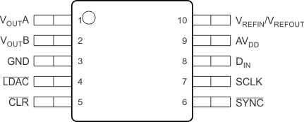
DGS Package
10-Pin VSSOP
(Top View)
DAC7562 DAC7563 DAC8162 DAC8163 DAC8562 DAC8563 po-DGS_las719.gif
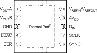
DSC Package
10-Pin WSON With Thermal Pad
(Top View)
DAC7562 DAC7563 DAC8162 DAC8163 DAC8562 DAC8563 po-DSC_SLAS719.gif
1. TI recommends connecting the thermal pad to the ground plane for better thermal dissipation.

Pin Functions

PIN I/O DESCRIPTION
NAME NO.
AVDD 9 I Power-supply input, 2.7 V to 5.5 V
CLR 5 I Asynchronous clear input. The CLR input is falling-edge sensitive. On activation of CLR, zero scale (DACxx62) or mid-scale (DACxx63) is loaded to all input and DAC registers. This sets the DAC output voltages accordingly. The device exits clear code mode on the 24th falling edge of the next write to the device. Activating CLR during a write sequence aborts the write.
DIN 8 I Serial data input. Data are clocked into the 24-bit input shift register on each falling edge of the serial clock input. Schmitt-trigger logic input
GND 3 Ground reference point for all circuitry on the device
LDAC 4 I In synchronous mode, data update occurs with the falling edge of the 24th SCLK cycle, which follows a falling edge of SYNC. Such synchronous updates do not require the LDAC, which must be connected to GND permanently or asserted and held low before sending commands to the device.
In asynchronous mode, the LDAC pin is used as a negative edge-triggered timing signal for simultaneous DAC updates. Multiple single-channel commands can be written in order to set different channel buffers to desired values and then make a falling edge on the LDAC pin to update the DAC output registers simultaneously.
SCLK 7 I Serial clock input. Data can be transferred at rates up to 50 MHz. Schmitt-trigger logic input
SYNC 6 I Level-triggered control input (active-low). This input is the frame synchronization signal for the input data. When SYNC goes low, it enables the input shift register, and data are sampled on subsequent falling clock edges. The DAC output updates following the 24th clock falling edge. If SYNC is taken high before the 23rd clock edge, the rising edge of SYNC acts as an interrupt, and the write sequence is ignored by the DAC756x, DAC816x, and DAC856x devices. Schmitt-trigger logic input
VOUTA 1 O Analog output voltage from DAC-A
VOUTB 2 O Analog output voltage from DAC-B
VREFIN/VREFOUT 10 I/O Bidirectional voltage reference pin. If internal reference is used, 2.5-V output.