JAJSEF1D December 2013 – December 2021 DAC7750 , DAC8750
PRODUCTION DATA
- 1 特長
- 2 アプリケーション
- 3 概要
- 4 Revision History
- 5 Device Comparison Table
- 6 Pin Configuration and Functions
- 7 Specifications
- 8 Detailed Description
- 9 Application and Implementation
- 10Power Supply Recommendations
- 11Layout
- 12Device and Documentation Support
- 13Mechanical, Packaging, and Orderable Information
パッケージ・オプション
メカニカル・データ(パッケージ|ピン)
サーマルパッド・メカニカル・データ
発注情報
8.3.6 Power-On Reset
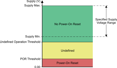
The DACx750 incorporates two internal POR circuits for the DVDD and AVDD supplies. The DVDD and AVDD POR signals are ANDed together so that both supplies must be at their minimal specified values for the device to not be in a reset condition. These POR circuits initialize internal logic and registers, as well as set the analog outputs to a known state while the device supplies are ramping. All registers are reset to their default values. Typically the POR function can be ignored, as long as the device supplies power-up and maintains the specified minimum voltage levels. However, in the case of a supply drop or brownout, the DACx750 can have an internal POR reset event or lose digital memory integrity. Figure 8-3 represents the threshold levels for the internal POR for both the DVDD and AVDD supplies.
 Figure 8-3 Relevant Voltage Levels for POR Circuit
For the DVDD supply, no internal POR occurs for nominal supply operation from 2.7 V (supply min) to 5.5 V (supply max). For the DVDD supply region between 2.4 V (undefined operation threshold) and 0.8 V (POR threshold), the internal POR circuit may or may not provide a reset over all temperature conditions. For the DVDD supply below 0.8 V (POR threshold), the internal POR resets if the supply voltage remains less than 0.8 V for approximately 1 ms.
For the AVDD supply, no internal POR occurs for nominal supply operation from 10 V (supply min) to 36 V (supply max). For AVDD supply voltages between 8 V (undefined operation threshold) and 1 V (POR threshold), the internal POR circuit may or may not provide a reset over all temperature conditions. For the AVDD supply below 1 V (POR threshold), the internal POR resets if the supply voltage remains less than 1 V for approximately 1 ms. In case the DVDD or AVDD supply drops to a level where the internal POR signal is indeterminate, either power cycle the device, or toggle the LATCH pin and then perform a software reset. Both options initialize the internal circuitry to a known state and provide proper operation.