-
DAC8811 16-Bit, Serial Input Multiplying Digital-to-Analog Converter
- 1 Features
- 2 Applications
- 3 Description
- 4 Revision History
- 5 Device Comparison Table
- 6 Pin Configuration and Functions
- 7 Specifications
- 8 Detailed Description
- 9 Application and Implementation
- 10Power Supply Recommendations
- 11Layout
- 12Device and Documentation Support
- 13Mechanical, Packaging, and Orderable Information
- IMPORTANT NOTICE
パッケージ・オプション
メカニカル・データ(パッケージ|ピン)
サーマルパッド・メカニカル・データ
- DRB|8
発注情報
DAC8811 16-Bit, Serial Input Multiplying Digital-to-Analog Converter
1 Features
- ±0.5 LSB DNL
- 16-Bit Monotonic
- ±1 LSB INL
- Low Noise: 12 nV/√Hz
- Low Power: IDD = 2 µA
- 2.7-V to 5.5-V Analog Power Supply
- 2-mA Full-Scale Current ±20%,
with VREF = 10 V - 50-MHz Serial Interface
- 0.5-μs Settling Time
- 4-Quadrant Multiplying Reference
- Reference Bandwidth: 10 MHz
- ±10-V Reference Input
- Reference Dynamics: –105 THD
- Tiny 8-Lead 3 × 3 mm VSON and 3 × 5 mm VSSOP Packages
- Industry-Standard Pin Configuration
2 Applications
- Automatic Test Equipment
- Instrumentation
- Digitally Controlled Calibration
- Industrial Control PLCs
3 Description
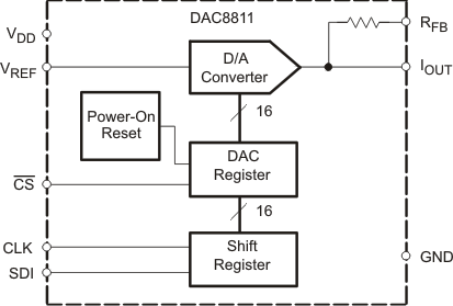
The DAC8811 multiplying digital-to-analog converter (DAC) is designed to operate from a single 2.7-V to 5.5-V supply.
The applied external reference input voltage VREF determines the full-scale output current. An internal feedback resistor (RFB) provides temperature tracking for the full-scale output when combined with an external I-to-V precision amplifier.
A serial data interface offers high-speed, three-wire microcontroller-compatible inputs using data-in (SDI), clock (CLK), and chip-select (CS).
On power-up, the DAC register is filled with zeroes, and the DAC output is at zero scale.
The DAC8811 is packaged in space-saving 8-lead VSON and VSSOP packages.
Device Information(1)
| PART NUMBER | PACKAGE | BODY SIZE (NOM) |
|---|---|---|
| DAC8811 | VSSOP (8) | 3.00 mm × 3.00 mm |
| VSON (8) | 3.00 mm × 3.00 mm |
- For all available packages, see the orderable addendum at the end of the datasheet.
4 Revision History
Changes from C Revision (October 2015) to D Revision
- Changed the DAC8811 Timing Diagram image to show the setup and hold time with respect to rising edge Go
- Changed two instances of falling to rising in the DAC8811 Input Shift Register sectionGo
- Changed the SYNC Interrupt Facility imageGo
Changes from B Revision (February 2007) to C Revision
- Added ESD Ratings table, Recommended Operating Conditions table, Thermal Information table, Timing Requirements table, Feature Description section, Device Functional Modes, Application and Implementation section, Power Supply Recommendations section, Layout section, Device and Documentation Support section, and Mechanical, Packaging, and Orderable Information sections. Go
- Changed R3' From: 50 kΩ To: 50 Ω in Figure 23Go
Changes from A Revision (December 2004) to B Revision
- Added a new paragraph to the Description, "On power-up,..."Go
- Changed the Simplified Schematic to include the Power-On ResetGo
- Added VREF, RFB to GND to the Absolute Maximum RatingsGo
- Changed the ESD rating of HBM From: 1500 To: 4000 in the Absolute Maximum RatingsGo
- Added table note: " All ac characteristic tests are performed.." to the Electrical CharacteristicsGo
- Added test conditions to the Output voltage settling time of the AC characteristics section in the Timing Requirements Go
- Changed Figure 9Go
Changes from * Revision (November 2004) to A Revision
- Removed the Product Preview labelGo
- Added information to the Features Go
- Added Output leakage current Data = 0000h, TA = TMAX in the Electrical Characteristics Go
- Added Input high voltage for VDD = 2.7 V and 2.5 V in the Electrical Characteristics Go
- Changed the values of the Power Requirements and the AC characteristics section in the Electrical Characteristics Go
5 Device Comparison Table
| PART NUMBER | INL (LSB) | DNL (LSB) |
|---|---|---|
| DAC8811ICDGK | ±1 | ±1 |
| DAC8811IBDGK | ±2 | ±1 |
| DAC8811ICDRB | ±1 | ±1 |
| DAC8811IBDRB | ±2 | ±1 |
