SLAS411D November 2004 – February 2016 DAC8811
PRODUCTION DATA.
- 1 Features
- 2 Applications
- 3 Description
- 4 Revision History
- 5 Device Comparison Table
- 6 Pin Configuration and Functions
- 7 Specifications
- 8 Detailed Description
- 9 Application and Implementation
- 10Power Supply Recommendations
- 11Layout
- 12Device and Documentation Support
- 13Mechanical, Packaging, and Orderable Information
パッケージ・オプション
メカニカル・データ(パッケージ|ピン)
サーマルパッド・メカニカル・データ
- DRB|8
発注情報
8 Detailed Description
8.1 Overview
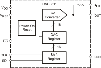
The DAC8811 is a single channel current output, 16-bit digital-to-analog converter (DAC). The device includes a 3-wire serial interface to communicate with most DSPs.
8.2 Functional Block Diagram
8.3 Feature Description
The DAC8811 is a single channel current output, 16-bit digital-to-analog converter (DAC). The architecture, illustrated in Figure 18, is an R-2R ladder configuration with the three MSBs segmented. Each 2R leg of the ladder is either switched to GND or the IOUT terminal. The IOUT terminal of the DAC is held at a virtual GND potential by the use of an external I/V converter op amp. The R-2R ladder is connected to an external reference input VREF that determines the DAC full-scale current. The R-2R ladder presents a code independent load impedance to the external reference of 5 kΩ ±25%. The external reference voltage can vary in a range of -15 V to 15 V, thus providing bipolar IOUT current operation. By using an external I/V converter and the DAC8811 RFB resistor, output voltage ranges of -VREF to VREF can be generated.
 Figure 18. Equivalent R-2R DAC Circuit
When using an external I/V converter and the DAC8811 RFB resistor, the DAC output voltage is given by Equation 1:

Each DAC code determines the 2R leg switch position to either GND or IOUT. Because the DAC output impedance as seen looking into the IOUT terminal changes versus code, the external I/V converter noise gain will also change. Because of this, the external I/V converter op amp must have a sufficiently low offset voltage such that the amplifier offset is not modulated by the DAC IOUT terminal impedance change. External op amps with large offset voltages can produce INL errors in the transfer function of the DAC8811 due to offset modulation versus DAC code. For best linearity performance of the DAC8811, an operational amplifier (OPA277) is recommended (Figure 19). This circuit allows VREF swinging from -10 V to +10 V.
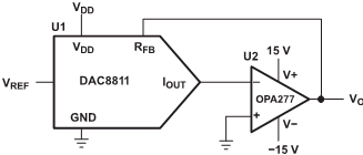 Figure 19. Voltage Output Configuration
8.3.1 Stability Circuit
For a current-to-voltage design (see Figure 20), the DAC8811 current output (IOUT) and the connection with the inverting node of the op amp should be as short as possible and according to correct PCB layout design. For each code change, there is a step function. If the GBP of the op amp is limited and parasitic capacitance is excessive at the inverting node then gain peaking is possible. Therefore, for circuit stability, a compensation capacitor C1 (4 pF to 20 pF typ) can be added to the design, as shown in Figure 20.
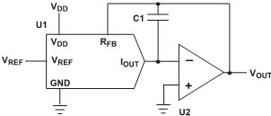 Figure 20. Gain Peaking Prevention Circuit With Compensation Capacitor
8.3.2 Positive Voltage Output Circuit
As Figure 21 illustrates, in order to generate a positive voltage output, a negative reference is input to the DAC8811. This design is suggested instead of using an inverting amp to invert the output due to tolerance errors of the resistor. For a negative reference, VOUT and GND of the reference are level-shifted to a virtual ground and a –2.5 V input to the DAC8811 with an op amp.
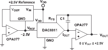 Figure 21. Positive Voltage Output Circuit
8.3.3 Bipolar Output Circuit
The DAC8811, as a 2-quadrant multiplying DAC, can be used to generate a unipolar output. The polarity of the full-scale output IOUT is the inverse of the input reference voltage at VREF.
Some applications require full 4-quadrant multiplying capabilities or bipolar output swing. As shown in Figure 22, external op amp U4 is added as a summing amp and has a gain of 2X that widens the output span to 5 V. A 4-quadrant multiplying circuit is implemented by using a 2.5-V offset of the reference voltage to bias U4. According to the circuit transfer equation given in Equation 2, input data (D) from code 0 to full scale produces output voltages of VOUT = -2.5 V to VOUT = +2.5 V.

External resistance mismatching is the significant error in Figure 22.
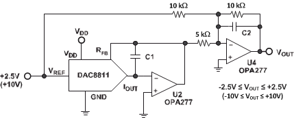 Figure 22. Bipolar Output Circuit
8.3.4 Programmable Current Source Circuit
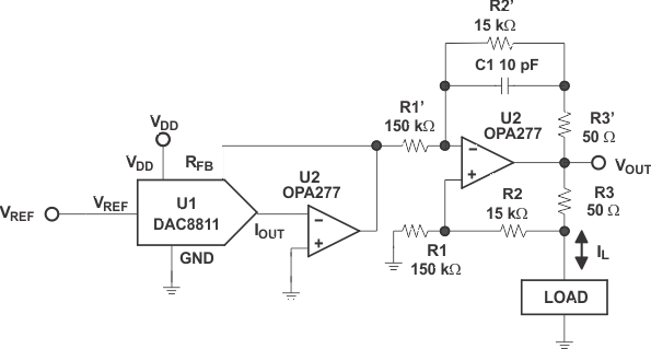
A DAC8811 can be integrated into the circuit in Figure 23 to implement an improved Howland current pump for precise voltage to current conversions. Bidirectional current flow and high voltage compliance are two features of the circuit. With a matched resistor network, the load current of the circuit is shown by Equation 3:

The value of R3 in the previous equation can be reduced to increase the output current drive of U3. U3 can drive ±20 mA in both directions with voltage compliance limited up to 15 V by the U3 voltage supply. Elimination of the circuit compensation capacitor C1 in the circuit is not suggested as a result of the change in the output impedance ZO, according to Equation 4:

As shown in Equation 4, with matched resistors, ZO is infinite and the circuit is optimum for use as a current source. However, if unmatched resistors are used, ZO is positive or negative with negative output impedance being a potential cause of oscillation. Therefore, by incorporating C1 into the circuit, possible oscillation problems are eliminated. The value of C1 can be determined for critical applications; for most applications, however, a value of several pF is suggested.
8.4 Device Functional Mode
Table 1. Control Logic Truth Table(1)
| CLK | CS | SERIAL SHIFT REGISTER | DAC REGISTER |
|---|---|---|---|
| X | H | No effect | Latched |
| ↑+ | L | Shift register data advanced one bit | Latched |
| X | H | No effect | Latched |
| X | ↑+ | Shift register data transferred to DAC register | New data loaded from serial register |
8.5 Programming
8.5.1 DAC8811 Input Shift Register
The DAC8811 has a 3-wire serial interface (CS, SCLK, and DIN) compatible with SPI, QSPI, and Microwire interface standards, as well as most DSPs. See Figure 1 for an example of a typical write sequence.
The input shift register is 16 bits wide, as shown in Figure 25. The write sequence begins by bringing the CS line low. Data from the DIN line are clocked into the 16-bit shift register on each rising edge of CLK. The serial clock frequency can be as high as 50 MHz, making the DAC8811 compatible with high-speed DSPs. On the 16th rising edge of the serial clock, the last data bit is clocked in and the programmed function is executed.
At this point, the CS line may be kept low or brought high. In either case, it must be brought high for a minimum of 20 ns before the next write sequence so that a falling edge of CS can initiate the next write sequence.
| DB15 | DB0 | ||||||||||||||
| D15 | D15 | D13 | D12 | D11 | D10 | D9 | D8 | D7 | D6 | D5 | D4 | D3 | D2 | D1 | D0 |
| LEGEND: R/W = Read/Write; R = Read only; -n = value after reset |
