JAJS261B July   2007  – January 2018 DAC8881

PRODUCTION DATA.  

  1. 特長
  2. アプリケーション
  3. 概要
    1.     Device Images
      1.      ブロック図
  4. 改訂履歴
  5. Pin Configuration and Functions
    1.     Pin Functions
  6. Specifications
    1. 6.1 Absolute Maximum Ratings
    2. 6.2 ESD Ratings
    3. 6.3 Recommended Operating Conditions
    4. 6.4 Thermal Information
    5. 6.5 Electrical Characteristics
    6. 6.6 Timing Characteristics for
    7. 6.7 Timing Characteristics for and
    8. 6.8 Typical Characteristics: VDD = +5 V
    9. 6.9 TYpical Characteristics: VDD = +2.7 V
  7. Detailed Description
    1. 7.1 Overview
    2. 7.2 Functional Block Diagram
    3. 7.3 Feature Description
      1. 7.3.1  Analog Output
      2. 7.3.2  Reference Inputs
      3. 7.3.3  Output Range
      4. 7.3.4  Input Data Format
      5. 7.3.5  Hardware Reset
      6. 7.3.6  Power-On Reset
      7. 7.3.7  Program Reset Value
      8. 7.3.8  Power Down
      9. 7.3.9  Double-Buffered Interface
      10. 7.3.10 Load DAC Pin (LDAC)
        1. 7.3.10.1 Synchronous Mode
        2. 7.3.10.2 Asynchronous Mode
      11. 7.3.11 1.8 V to 5.5 V Logic Interface
    4. 7.4 Device Functional Modes
      1. 7.4.1 Serial Interface
        1. 7.4.1.1 Input Shift Register
          1. 7.4.1.1.1 Stand-Alone Mode
          2. 7.4.1.1.2 Daisy-Chain Mode
  8. Application and Implementation
    1. 8.1 Application Information
      1. 8.1.1 Bipolar Operation Using The DAC8881
    2. 8.2 Typical Application
      1. 8.2.1 DAC8881 Sample Hold Circuit
        1. 8.2.1.1 Design Requirements
        2. 8.2.1.2 Detailed Design Procedure
        3. 8.2.1.3 Application Curves
    3. 8.3 System Example
  9. Power Supply Recommendations
  10. 10Layout
    1. 10.1 Layout Guidelines
    2. 10.2 Layout Example
  11. 11デバイスおよびドキュメントのサポート
    1. 11.1 ドキュメントのサポート
      1. 11.1.1 関連資料
    2. 11.2 ドキュメントの更新通知を受け取る方法
    3. 11.3 コミュニティ・リソース
    4. 11.4 商標
    5. 11.5 静電気放電に関する注意事項
    6. 11.6 Glossary

パッケージ・オプション

メカニカル・データ(パッケージ|ピン)
サーマルパッド・メカニカル・データ
発注情報

Analog Output

The DAC8881 offers a force and sense output configuration for the high open-loop gain output amplifier. This feature allows the loop around the output amplifier to be closed at the load (as shown in Figure 68), thus ensuring an accurate output voltage. The output buffer VOUT and RFB pins are provided so that the output op amp buffer feedback can be connected at the load. Without a driven load, the DAC8881 output typically swings to within 15mV of the AGND and AVDD supply rails. Because of the high accuracy of these DACs, system design problems such as grounding and contact resistance become very important. A 16-bit converter with a 5 V full-scale range has a 1 LSB value of 76 μV. With a load current of 1 mA, a series wiring and connector resistance of only 80mΩ (RW2) causes a voltage drop of 80 μV. In terms of a system layout, the resistivity of a typical 1-ounce copper-clad printed circuit board is 0.5mΩ per square. For a 1mA load, a 0.25 mm wide printed circuit conductor 25 mm long results in a voltage drop of 50 μV.
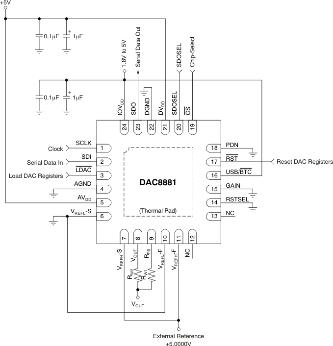
DAC8881 ai_analog_config_bas422.gifFigure 68. Analog Output Closed-Loop Configuration
(RW1 and RW2 represent wiring resistance)