JAJS261B July   2007  – January 2018 DAC8881

PRODUCTION DATA.  

  1. 特長
  2. アプリケーション
  3. 概要
    1.     Device Images
      1.      ブロック図
  4. 改訂履歴
  5. Pin Configuration and Functions
    1.     Pin Functions
  6. Specifications
    1. 6.1 Absolute Maximum Ratings
    2. 6.2 ESD Ratings
    3. 6.3 Recommended Operating Conditions
    4. 6.4 Thermal Information
    5. 6.5 Electrical Characteristics
    6. 6.6 Timing Characteristics for
    7. 6.7 Timing Characteristics for and
    8. 6.8 Typical Characteristics: VDD = +5 V
    9. 6.9 TYpical Characteristics: VDD = +2.7 V
  7. Detailed Description
    1. 7.1 Overview
    2. 7.2 Functional Block Diagram
    3. 7.3 Feature Description
      1. 7.3.1  Analog Output
      2. 7.3.2  Reference Inputs
      3. 7.3.3  Output Range
      4. 7.3.4  Input Data Format
      5. 7.3.5  Hardware Reset
      6. 7.3.6  Power-On Reset
      7. 7.3.7  Program Reset Value
      8. 7.3.8  Power Down
      9. 7.3.9  Double-Buffered Interface
      10. 7.3.10 Load DAC Pin (LDAC)
        1. 7.3.10.1 Synchronous Mode
        2. 7.3.10.2 Asynchronous Mode
      11. 7.3.11 1.8 V to 5.5 V Logic Interface
    4. 7.4 Device Functional Modes
      1. 7.4.1 Serial Interface
        1. 7.4.1.1 Input Shift Register
          1. 7.4.1.1.1 Stand-Alone Mode
          2. 7.4.1.1.2 Daisy-Chain Mode
  8. Application and Implementation
    1. 8.1 Application Information
      1. 8.1.1 Bipolar Operation Using The DAC8881
    2. 8.2 Typical Application
      1. 8.2.1 DAC8881 Sample Hold Circuit
        1. 8.2.1.1 Design Requirements
        2. 8.2.1.2 Detailed Design Procedure
        3. 8.2.1.3 Application Curves
    3. 8.3 System Example
  9. Power Supply Recommendations
  10. 10Layout
    1. 10.1 Layout Guidelines
    2. 10.2 Layout Example
  11. 11デバイスおよびドキュメントのサポート
    1. 11.1 ドキュメントのサポート
      1. 11.1.1 関連資料
    2. 11.2 ドキュメントの更新通知を受け取る方法
    3. 11.3 コミュニティ・リソース
    4. 11.4 商標
    5. 11.5 静電気放電に関する注意事項
    6. 11.6 Glossary

パッケージ・オプション

メカニカル・データ(パッケージ|ピン)
サーマルパッド・メカニカル・データ
発注情報

Application Curves

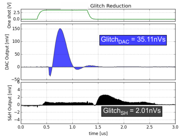
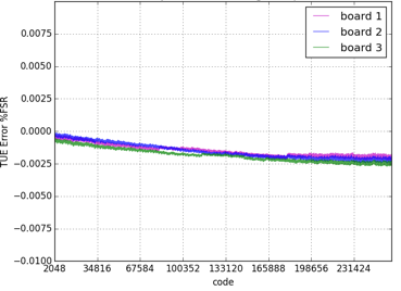
Glitch reduction and total unadjusted error (TUE) plots of the solution presented in Sample & Hold Glitch Reduction for Precision Outputs Design Guide (TIDU022) is shown in the following plots. The glitch area is reduced from 35.11 nVs to 2.01 nVs.
DAC8881 fig_24_sbas422.gif
Figure 75. DAC8881 Sample and Hold TUE Error %FSR
DAC8881 fig_33_sbas337.png
CH = 8.2 nF RS = 14.7 Ω
Figure 76. Measured Glitch Area
(20000h-1FFFFh 18-bit Data)
(Top) Digital Signal One-Shot Pulse; (Middle) DAC Output Glitch; (Bottom) S&H Output Glitch