JAJSI70C May 2008 – November 2019 DAC9881
PRODUCTION DATA.
- 1 特長
- 2 アプリケーション
- 3 概要
- 4 改訂履歴
- 5 概要(続き)
- 6 Pin Configuration and Functions
-
7 Specifications
- 7.1 Absolute Maximum Ratings
- 7.2 ESD Ratings
- 7.3 Recommended Operating Conditions
- 7.4 Thermal Information
- 7.5 Electrical Characteristics: AVDD = 5 V
- 7.6 Electrical Characteristics: AVDD = 2.7 V
- 7.7 Timing Requirements—Standalone Operation Without SDO
- 7.8 Timing Requirements—Standalone Operation With SDO and Daisy-Chain Mode
- 7.9 Typical Characteristics: AVDD = 5 V
- 7.10 Typical Characteristics: AVDD = 2.7 V
-
8 Detailed Description
- 8.1 Overview
- 8.2 Functional Block Diagram
- 8.3 Feature Description
- 8.4 Device Functional Modes
- 9 Application and Implementation
- 10Power Supply Recommendations
- 11Layout
- 12デバイスおよびドキュメントのサポート
- 13メカニカル、パッケージ、および注文情報
パッケージ・オプション
メカニカル・データ(パッケージ|ピン)
- RGE|24
サーマルパッド・メカニカル・データ
- RGE|24
発注情報
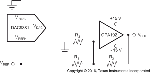
9.1.1 Bipolar Operation Using the DAC9881
The DAC9881 is designed for single-supply operation; however, a bipolar output is also possible using the circuit shown in Figure 70. This circuit gives a bipolar output voltage of VOUT. When GAIN = 1, VOUT can be calculated using Equation 2:

Some pins are omitted for clarity.
Figure 70. Bipolar Output Range Equation 2. 

where
- VOUT(CODE) = output voltage vs code
- CODE = 0 to 262143. This is the digital code loaded to the DAC
- VREF = reference voltage applied to the DAC9881
As an example, a ±8-V output span can be achieved by using values of 5 V, 6.25 kΩ, 16.67 kΩ, and 10 kΩ for Vref, R1, R2, and R3 respectively.