JAJSI70C May 2008 – November 2019 DAC9881
PRODUCTION DATA.
- 1 特長
- 2 アプリケーション
- 3 概要
- 4 改訂履歴
- 5 概要(続き)
- 6 Pin Configuration and Functions
-
7 Specifications
- 7.1 Absolute Maximum Ratings
- 7.2 ESD Ratings
- 7.3 Recommended Operating Conditions
- 7.4 Thermal Information
- 7.5 Electrical Characteristics: AVDD = 5 V
- 7.6 Electrical Characteristics: AVDD = 2.7 V
- 7.7 Timing Requirements—Standalone Operation Without SDO
- 7.8 Timing Requirements—Standalone Operation With SDO and Daisy-Chain Mode
- 7.9 Typical Characteristics: AVDD = 5 V
- 7.10 Typical Characteristics: AVDD = 2.7 V
-
8 Detailed Description
- 8.1 Overview
- 8.2 Functional Block Diagram
- 8.3 Feature Description
- 8.4 Device Functional Modes
- 9 Application and Implementation
- 10Power Supply Recommendations
- 11Layout
- 12デバイスおよびドキュメントのサポート
- 13メカニカル、パッケージ、および注文情報
パッケージ・オプション
メカニカル・データ(パッケージ|ピン)
- RGE|24
サーマルパッド・メカニカル・データ
- RGE|24
発注情報
9.2.1.1 Design Requirements
The inherent architecture of the DAC9881, which consists of an R-2R architecture, enables great performance in regards to noise and accuracy, but at a cost of large glitch area. Glitch area, also known as glitch impulse area, is defined as the area associated with the overshoot or undershoot created by a code transition, and is generally quantified in Volt-seconds. Different code-to-code transitions produce different levels of glitch impulses. DACs with R-2R architectures produce large glitches during major-carry transitions.
There are two methods that can be used to reduce this glitch area:
- Add an external RC Filter to the output of the DAC.
- The low-pass filter helps attenuate high-frequency glitches that would normally propagate to the DAC output. Best practice is to use a small resistor value, as large resistance develops a large potential drop and reduces the voltage seen at the load. Capacitor values can be determined from the desired cutoff frequency of the low-pass filter, as well as settling time.
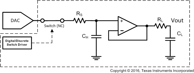
- Another technique is to employ a Sample and Hold (S&H) circuit following the DAC output.
- In its simplest form, the sample and hold circuit can be constructed from the following components: a capacitive element, output buffer, and switch. A schematic of the simplified S&H is shown in Figure 72.
 Figure 72. Simplified Sample and Hold Circuit