JAJSMO5C August 2000 – August 2021 DCV010505 , DCV010505D , DCV010512 , DCV010512D , DCV010515 , DCV010515D , DCV011512D , DCV011515D , DCV012405 , DCV012415D
PRODUCTION DATA
- 1 特長
- 2 アプリケーション
- 3 概要
- 4 Revision History
- 5 Device Comparison Table
- 6 Pin Configuration and Functions
- 7 Specifications
-
8 Detailed Description
- 8.1 Overview
- 8.2 Functional Block Diagrams
- 8.3 Feature Description
- 8.4 Device Functional Modes
-
9 Application and Implementation
- 9.1 Application Information
- 9.2
Typical Application
- 9.2.1 Design Requirements
- 9.2.2 Detailed Design Procedure
- 9.2.3 Application Curves
- 10Power Supply Recommendations
- 11Layout
- 12Device and Documentation Support
- 13Mechanical, Packaging, and Orderable Information
パッケージ・オプション
メカニカル・データ(パッケージ|ピン)
サーマルパッド・メカニカル・データ
発注情報
8.3.10 Power-Up Characteristics
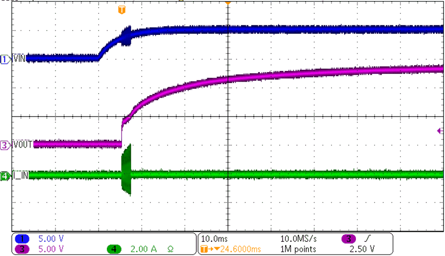
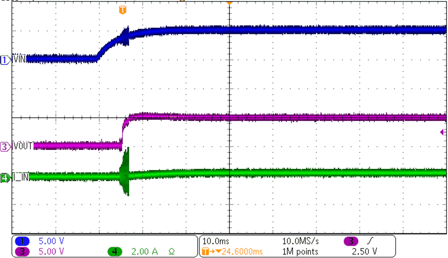
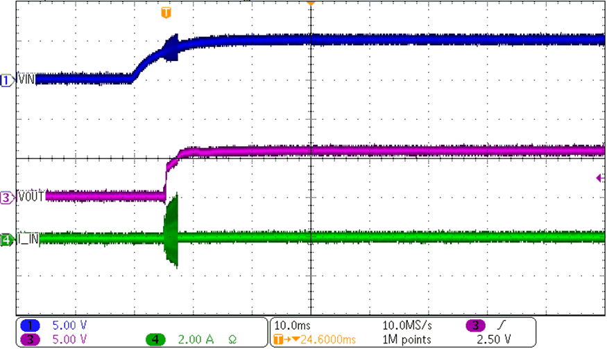
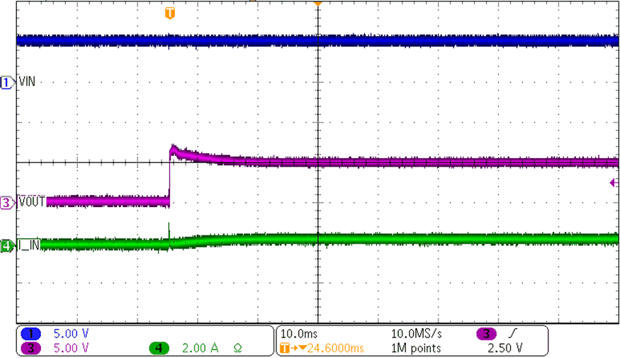
The DCV01 series of devices do not include a soft-start feature. Therefore, a high in-rush current during power-up is expected. To ensure a more stable start-up, allow the input voltage to be in regulation before enabling the device. Refer to the Section 8.4.1 section on how to disable/enable the device. Figure 8-6 shows the typical start-up waveform for a DCV010505P when enabled after the input voltage is in regulation. Figure 8-3 shows the typical start-up waveform for a DCV010505P, operating from a 5-V input with no load on the output. Figure 8-4 shows the start-up waveform for a DCV010505P starting up into a 10% load. Figure 8-5 shows the start-up waveform starting up into a full (100%) load.
 Figure 8-3 DCV010505P Start-Up at No Load
 Figure 8-5 DCV010505P Start-Up at 100% Load
 Figure 8-4 DCV010505P Start-Up at 10% Load
 Figure 8-6 DCV010505P Enable Start-Up at 100% Load