JAJSPI5B December   2022  – August 2024 DLP4621-Q1

PRODUCTION DATA  

  1.   1
  2. 特長
  3. アプリケーション
  4. 概要
  5. Pin Configuration and Functions
  6. Specifications
    1. 5.1  Absolute Maximum Ratings
    2. 5.2  Storage Conditions
    3. 5.3  ESD Ratings
    4. 5.4  Recommended Operating Conditions
      1. 5.4.1 Illumination Overfill Diagram
    5. 5.5  Thermal Information
    6. 5.6  Electrical Characteristics
    7. 5.7  Timing Requirements
      1.      Electrical and Timing Diagrams
    8. 5.8  Switching Characteristics
      1. 5.8.1 LPSDR and Test Load Circuit Diagrams
    9. 5.9  System Mounting Interface Loads
      1.      System Interface Loads Diagram
    10. 5.10 Micromirror Array Physical Characteristics
      1. 5.10.1 Micromirror Array Physical Characteristics Diagram
    11. 5.11 Micromirror Array Optical Characteristics
    12. 5.12 Window Characteristics
    13. 5.13 Chipset Component Usage Specification
  7. Detailed Description
    1. 6.1 Overview
    2. 6.2 Functional Block Diagram
    3. 6.3 Feature Description
      1. 6.3.1 SubLVDS Data Interface
      2. 6.3.2 Low Speed Interface for Control
      3. 6.3.3 DMD Voltage Supplies
      4. 6.3.4 Asynchronous Reset
      5. 6.3.5 Temperature Sensing Diode
        1. 6.3.5.1 Temperature Sense Diode Theory
    4. 6.4 System Optical Considerations
      1. 6.4.1 Numerical Aperture and Stray Light Control
      2. 6.4.2 Pupil Match
      3. 6.4.3 Illumination Overfill
    5. 6.5 DMD Image Performance Specification
    6. 6.6 Micromirror Array Temperature Calculation
      1. 6.6.1 Monitoring Array Temperature Using the Temperature Sense Diode
    7. 6.7 Micromirror Landed-On/Landed-Off Duty Cycle
      1. 6.7.1 Definition of Micromirror Landed-On/Landed-Off Duty Cycle
  8. Application and Implementation
    1. 7.1 Application Information
    2. 7.2 Typical Application
      1. 7.2.1 Application Overview
      2. 7.2.2 Input Image Resolution
      3. 7.2.3 Reference Design
      4. 7.2.4 Application Mission Profile Consideration
    3. 7.3 Power Supply Recommendations
      1. 7.3.1 Power Supply Power-Up Procedure
      2. 7.3.2 Power Supply Power-Down Procedure
      3. 7.3.3 Power Supply Sequencing Requirements
    4. 7.4 Layout Guidelines
    5. 7.5 Layout Example
  9. Device and Documentation Support
    1. 8.1 Device Support
      1. 8.1.1 Device Nomenclature
      2. 8.1.2 Device Markings
    2. 8.2 サード・パーティ製品に関する免責事項
    3. 8.3 ドキュメントの更新通知を受け取る方法
    4. 8.4 サポート・リソース
    5. 8.5 Trademarks
    6. 8.6 静電気放電に関する注意事項
    7. 8.7 DMD Handling
    8. 8.8 用語集
  10. Revision History
  11. 10Mechanical, Packaging, and Orderable Information

パッケージ・オプション

デバイスごとのパッケージ図は、PDF版データシートをご参照ください。

メカニカル・データ(パッケージ|ピン)
  • FQX|120
サーマルパッド・メカニカル・データ
発注情報

Temperature Sense Diode Theory

A temperature-sensing diode is based on the fundamental current and temperature characteristics of a transistor. The diode is formed by connecting the transistor base to the collector. Three different known currents flow through the diode and the resulting diode voltage is measured in each case. The difference in their base-emitter voltages is proportional to the absolute temperature of the transistor.

Refer to the TMP411-Q1 data sheet for detailed information about temperature diode theory and measurement. Figure 6-2 and Figure 6-3 illustrate the relationships between the current and voltage through the diode.
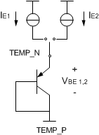
DLP4621-Q1 Temperature Measurement TheoryFigure 6-2 Temperature Measurement Theory
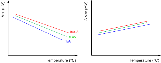
DLP4621-Q1 Example of Delta VBE
                    Versus TemperatureFigure 6-3 Example of Delta VBE Versus Temperature