JAJSPI5B December 2022 – August 2024 DLP4621-Q1
PRODUCTION DATA
- 1
- 1 特長
- 2 アプリケーション
- 3 概要
- 4 Pin Configuration and Functions
-
5 Specifications
- 5.1 Absolute Maximum Ratings
- 5.2 Storage Conditions
- 5.3 ESD Ratings
- 5.4 Recommended Operating Conditions
- 5.5 Thermal Information
- 5.6 Electrical Characteristics
- 5.7 Timing Requirements
- 5.8 Switching Characteristics
- 5.9 System Mounting Interface Loads
- 5.10 Micromirror Array Physical Characteristics
- 5.11 Micromirror Array Optical Characteristics
- 5.12 Window Characteristics
- 5.13 Chipset Component Usage Specification
- 6 Detailed Description
- 7 Application and Implementation
- 8 Device and Documentation Support
- 9 Revision History
- 10Mechanical, Packaging, and Orderable Information
パッケージ・オプション
デバイスごとのパッケージ図は、PDF版データシートをご参照ください。
メカニカル・データ(パッケージ|ピン)
- FQX|120
サーマルパッド・メカニカル・データ
発注情報
6.6 Micromirror Array Temperature Calculation
 Figure 6-4 DMD
Thermal Test Points
Figure 6-4 DMD
Thermal Test PointsThe active array temperature can be computed analytically from the thermal measurement point on the outside of the package, the package thermal resistance, the electrical power, and the illumination heat load. The relationship between array temperature and the reference ceramic temperature (TP1) in Figure 6-4 is provided by the following equations:
where
- TARRAY = computed array temperature (°C)
- TCERAMIC = measured ceramic temperature at the TP1 location in Figure 6-4 (°C)
- RARRAY–TO–CERAMIC = DMD package
thermal resistance from array to thermal test point TP1 (°C/W),
- QARRAY = total power (electrical plus absorbed) on the DMD array (W)
- QELECTRICAL = nominal electrical power dissipation by the DMD (W)
- QILLUMINATION = absorbed illumination heat load (W)
- QINCIDENT = incident power on the DMD (W)
The DMD absorption constant is a function of illumination distribution on the active array and the array border, angle of incidence (AOI), f number of the system, and operating state of the mirrors. The absorption constant is higher in the OFF state than in the ON state. Equations to calculate the absorption constant are provided for both ON and OFF mirror states. They assume an AOI of 34 degrees, an f/1.7 system, and they account for the distribution of light on the active array, POM, and array border.
Electrical power dissipation of the DMD is variable and depends on the voltages, data rates, and operating frequencies.
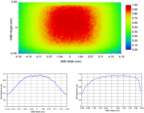
The DMD package thermal resistance from array to ceramic (RARRAY–TO–CERAMIC) assumes a non-uniform illumination distribution on the DMD as shown in Non-Uniform Illumination Profile figure. For illumination profiles more uniform than the one highlighted in Non-Uniform Illumination Profile figure, the value provided here is valid. However, for more non-uniform profiles (for example, Gaussian distribution) the thermal resistance will be higher. Please contact TI to determine an accurate value for this case.
 Figure 6-5 Non-Uniform Illumination Profile
The following sample calculations assume 10% of the total incident light falls outside of the active array and POM, and the mirrors are in the OFF state.
- TCERAMIC = 50°C (measured)
- QINCIDENT = 10W (measured)
- DMD Absorption Constant = 0.895 – 0.004783 × 90 = 0.46
- QELECTRICAL = 0.4W
- RARRAY–TO–CERAMIC = 1.5°C/W
- QARRAY = 0.4W + (0.46 x 10 W) = 5W
- TARRAY = 50°C × (5W x 1.5°C/W) = 57.5°C
When designing the DMD heatsink solution, the package thermal resistance from array to reference ceramic temperature (thermocouple location TP1 can be used to determine the temperature rise through the package as given by the following equations: