JAJSI71C April   2019  – February 2023 DLP470NE

PRODUCTION DATA  

  1. 特長
  2. アプリケーション
  3. 概要
  4. Revision History
  5. Pin Configuration and Functions
  6. Specifications
    1. 6.1  Absolute Maximum Ratings
    2. 6.2  Storage Conditions
    3. 6.3  ESD Ratings
    4. 6.4  Recommended Operating Conditions
    5. 6.5  Thermal Information
    6. 6.6  Electrical Characteristics
    7. 6.7  Capacitance at Recommended Operating Conditions
    8. 6.8  Timing Requirements
    9. 6.9  System Mounting Interface Loads
    10. 6.10 Micromirror Array Physical Characteristics
    11. 6.11 Micromirror Array Optical Characteristics
    12. 6.12 Window Characteristics
    13. 6.13 Chipset Component Usage Specification
  7. Detailed Description
    1. 7.1 Overview
    2. 7.2 Functional Block Diagram
    3. 7.3 Feature Description
      1. 7.3.1 Power Interface
      2. 7.3.2 Timing
    4. 7.4 Device Functional Modes
    5. 7.5 Optical Interface and System Image Quality Considerations
      1. 7.5.1 Numerical Aperture and Stray Light Control
      2. 7.5.2 Pupil Match
      3. 7.5.3 Illumination Overfill
    6. 7.6 Micromirror Array Temperature Calculation
    7. 7.7 Micromirror Landed-On/Landed-Off Duty Cycle
      1. 7.7.1 Definition of Micromirror Landed-On/Landed-Off Duty Cycle
      2. 7.7.2 Landed Duty Cycle and Useful Life of the DMD
      3. 7.7.3 Landed Duty Cycle and Operational DMD Temperature
      4. 7.7.4 Estimating the Long-Term Average Landed Duty Cycle of a Product or Application
  8. Application and Implementation
    1. 8.1 Application Information
    2. 8.2 Typical Application
      1. 8.2.1 Design Requirements
      2. 8.2.2 Detailed Design Procedure
      3. 8.2.3 Application Curves
    3. 8.3 DMD Die Temperature Sensing
  9. Power Supply Recommendations
    1. 9.1 DMD Power Supply Power-Up Procedure
    2. 9.2 DMD Power Supply Power-Down Procedure
  10. 10Layout
    1. 10.1 Layout Guidelines
    2. 10.2 Layout Example
      1. 10.2.1 Layers
      2. 10.2.2 Impedance Requirements
      3. 10.2.3 Trace Width, Spacing
        1. 10.2.3.1 Voltage Signals
  11. 11Device and Documentation Support
    1. 11.1 サード・パーティ製品に関する免責事項
    2. 11.2 Device Support
      1. 11.2.1 Device Nomenclature
      2. 11.2.2 Device Markings
    3. 11.3 Documentation Support
      1. 11.3.1 Related Documentation
    4. 11.4 Receiving Notification of Documentation Updates
    5. 11.5 サポート・リソース
    6. 11.6 Trademarks
    7. 11.7 静電気放電に関する注意事項
    8. 11.8 用語集
      1.      Mechanical, Packaging, and Orderable Information

パッケージ・オプション

メカニカル・データ(パッケージ|ピン)
サーマルパッド・メカニカル・データ
発注情報

DMD Die Temperature Sensing

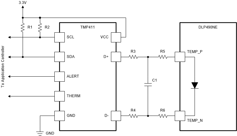
The DMD features a built-in thermal diode that measures the temperature at one corner of the die outside the micromirror array. The thermal diode can be interfaced with the TMP411 temperature sensor, as shown in Figure 8-3. The serial bus from the TMP411 can be connected to the DLPC4430 display controller to enable its temperature sensing features. See the DLPC4430 Programmers’ Guide for instructions on installing the DLPC4430 controller support firmware bundle and obtaining the temperature readings.

The software application contains functions to configure the TMP411 to read the DMD temperature sensor diode. This data can be leveraged to incorporate additional functionality in the overall system design such as adjusting illumination, fan speeds, and so forth. All communication between the TMP411 and the DLPC4430 controller will be completed using the I2C interface. The TMP411 connects to the DMD via pins B17 and B18, as outlined in Section 5.
GUID-A305F56D-FE56-4232-8213-8DC29AE9CD97-low.gif
Details omitted for clarity, see the TI Reference Design for connections to the DLPC4430 controller.
See the TMP411 data sheet for system board layout recommendation.
See the TMP411 data sheet and the TI reference design for suggested component values for R1, R2, R3, R4, and C1.
R5 = 0 Ω. R6 = 0 Ω. Zero-ohm resistors need to be located close to the DMD package pins.
Figure 8-3 TMP411 Sample Schematic