JAJSM59B September 2020 – April 2022 DLP471TE
PRODUCTION DATA
- 1 特長
- 2 アプリケーション
- 3 概要
- 4 Revision History
- 5 Pin Configuration and Functions
-
6 Specifications
- 6.1 Absolute Maximum Ratings
- 6.2 Storage Conditions
- 6.3 ESD Ratings
- 6.4 Recommended Operating Conditions
- 6.5 Thermal Information
- 6.6 Electrical Characteristics
- 6.7 Switching Characteristics
- 6.8 Timing Requirements
- 6.9 System Mounting Interface Loads
- 6.10 Micromirror Array Physical Characteristics
- 6.11 Micromirror Array Optical Characteristics
- 6.12 Window Characteristics
- 6.13 Chipset Component Usage Specification
- 7 Detailed Description
- 8 Application and Implementation
- 9 Power Supply Recommendations
- 10Layout
- 11Device and Documentation Support
- 12Mechanical, Packaging, and Orderable Information
7.7.4 Estimating the Long-Term Average Landed Duty Cycle of a Product or Application
During a given period of time, the landed duty cycle of a given pixel follows from the image content being displayed by that pixel.
For example, in the simplest case, when displaying pure-white on a given pixel for a given time period, that pixel operates under a 100/0 landed duty cycle during that time period. Likewise, when displaying pure-black, the pixel operates under a 0/100 landed duty cycle.
Between the two extremes (ignoring for the moment color and any image processing that may be applied to an incoming image), the landed duty cycle tracks one-to-one with the gray scale value, as shown in Table 7-1.
| GRAYSCALE VALUE | LANDED DUTY CYCLE | |||
|---|---|---|---|---|
| 0% | 0/100 | |||
| 10% | 10/90 | |||
| 20% | 20/80 | |||
| 30% | 30/70 | |||
| 40% | 40/60 | |||
| 50% | 50/50 | |||
| 60% | 60/40 | |||
| 70% | 70/30 | |||
| 80% | 80/20 | |||
| 90% | 90/10 | |||
| 100% | 100/0 | |||
Accounting for color rendition (but still ignoring image processing) requires knowing both the color intensity (from 0% to 100%) for each constituent primary color (red, green, and/or blue) for the given pixel as well as the color cycle time for each primary color, where “color cycle time” is the total percentage of the frame time that a given primary must be displayed in order to achieve the desired white point.
Use Equation 12 to calculate the landed duty cycle of a given pixel during a given time period
where
- Red_Cycle_%, represents the percentage of the frame time that red is displayed to achieve the desired white point
- Green_Cycle_% represents the percentage of the frame time that green is displayed to achieve the desired white point
- Blue_Cycle_%, represents the percentage of the frame time that blue is displayed to achieve the desired white point
For example, assume that the red, green, and blue color cycle times are 30%, 50%, and 20% respectively (in order to achieve the desired white point), then the landed duty cycle for various combinations of red, green, blue color intensities would be as shown in Table 7-2 and Table 7-3.
| CYCLE PERCENTAGE | ||
|---|---|---|
| RED | GREEN | BLUE |
| 30% | 50% | 20% |
| SCALE VALUE | LANDED DUTY CYCLE | |||
|---|---|---|---|---|
| RED | GREEN | BLUE | ||
| 0% | 0% | 0% | 0/100 | |
| 100% | 0% | 0% | 30/70 | |
| 0% | 100% | 0% | 50/50 | |
| 0% | 0% | 100% | 20/80 | |
| 0% | 12% | 0% | 6/94 | |
| 0% | 0% | 35% | 7/93 | |
| 60% | 0% | 0% | 18/82 | |
| 0% | 100% | 100% | 70/30 | |
| 100% | 0% | 100% | 50/50 | |
| 100% | 100% | 0% | 80/20 | |
| 0% | 12% | 35% | 13/87 | |
| 60% | 0% | 35% | 25/75 | |
| 60% | 12% | 0% | 24/76 | |
| 100% | 100% | 100% | 100/0 | |
The last factor to account for in estimating the landed duty cycle is any applied image processing. Within the DLPC7540 controller, the gamma function affects the landed duty cycle.
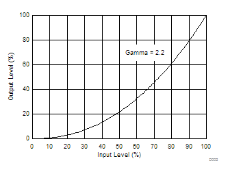
Gamma is a power function of the form Output_Level = A × Input_LevelGamma, where A is a scaling factor that is typically set to 1.
In the DLPC7540 controller, gamma is applied to the incoming image data on a pixel-by-pixel basis. A typical gamma factor is 2.2, which transforms the incoming data as shown in Figure 7-2.
 Figure 7-2 Example of Gamma = 2.2
From Figure 7-2, if the gray scale value of a given input pixel is 40% (before gamma is applied), then gray scale value is 13% after gamma is applied. Therefore, it can be seen that since gamma has a direct impact on the displayed gray scale level of a pixel, it also has a direct impact on the landed duty cycle of a pixel.
Consideration must also be given to any image processing which occurs before the DLPC7540 controllers.