JAJSUJ2 May 2024
ADVANCE INFORMATION
- 1
- 1 特長
- 2 アプリケーション
- 3 概要
- 4 Pin Configuration and Functions
-
5 Specifications
- 5.1 Absolute Maximum Ratings
- 5.2 Storage Conditions
- 5.3 ESD Ratings
- 5.4 Recommended Operating Conditions
- 11
- 12
- 5.5 Thermal Information
- 5.6 Electrical Characteristics
- 5.7 Switching Characteristics
- 5.8 Timing Requirements
- 5.9 System Mounting Interface Loads
- 5.10 Micromirror Array Physical Characteristics
- 5.11 Micromirror Array Optical Characteristics
- 5.12 Window Characteristics
- 5.13 Chipset Component Usage Specification
-
6 Detailed Description
- 6.1 Overview
- 6.2 Functional Block Diagram
- 6.3 Feature Description
- 6.4 Device Functional Modes
- 6.5 Optical Interface and System Image Quality Considerations
- 6.6 Micromirror Array Temperature Calculation
- 6.7 Micromirror Power Density Calculation
- 6.8 Window Aperture Illumination Overfill Calculation
- 6.9 Micromirror Landed-On/Landed-Off Duty Cycle
- 7 Application and Implementation
- 8 Power Supply Recommendations
- 9 Layout
- 10Device and Documentation Support
- 11Revision History
- 12Mechanical, Packaging, and Orderable Information
5.8 Timing Requirements
Over operating free-air temperature range and supply voltages (unless otherwise noted)
| PARAMETER | TEST CONDITIONS | MIN | TYP | MAX | UNIT | |
|---|---|---|---|---|---|---|
| LVCMOS | ||||||
| tr | Rise time(1) | 20% to 80% reference points | 25 | ns | ||
| tf | Fall time(1) | 80% to 20% reference points | 25 | ns | ||
| LOW SPEED INTERFACE (LSIF) | ||||||
| tr | Rise time(2) | 20% to 80% reference points | 450 | ps | ||
| tf | Fall time(2) | 80% to 20% reference points | 450 | ps | ||
| tW(H) | Pulse duration high(3) | LS_CLK. 50% to 50% reference points | 3.1 | ns | ||
| tW(L) | Pulse duration low(3) | LS_CLK. 50% to 50% reference points | 3.1 | ns | ||
| tsu | Setup time(4) | LS_WDATA valid before rising edge of LS_CLK (differential) | 1.5 | ns | ||
| th | Hold time(4) | LS_WDATA valid after rising edge of LS_CLK (differential) | 1.5 | ns | ||
| HIGH SPEED SERIAL INTERFACE (HSSI) | ||||||
| tr | Rise time(5)—data | from –A1 to A1 minimum eye height specification | 50 | 115 | ps | |
| Rise time(5)—clock | from –A1 to A1 minimum eye height specification | 50 | 135 | ps | ||
| tf | Fall time(5) - data | from A1 to –A1 minimum eye height specification | 50 | 115 | ps | |
| Fall time(5) - clock | from A1 to –A1 minimum eye height specification | 50 | 135 | ps | ||
| tW(H) | Pulse duration high(6) | DCLK. 50% to 50% reference points | 0.275 | ns | ||
| tW(L) | Pulse duration low(6) | DCLK. 50% to 50% reference points | 0.275 | ns | ||
(1) See Figure 5-10 for rise time and fall time for LVCMOS.
(2) See Figure 5-6 for rise time and fall time for LSIF.
(3) See Figure 5-5 for pulse duration high and low time for LSIF.
(4) See Figure 5-5 for setup and hold time for LSIF.
(5) See Figure 5-11 for rise time and fall time for HSSI.
(6) See Figure 5-13 for pulse duration high and low for HSSI.
Equation 1. 

Equation 2. 

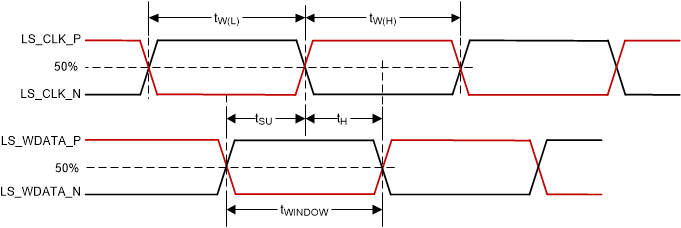 Figure 5-5 LSIF Timing
Requirements
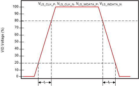 Figure 5-6 LSIF Rise, Fall Time
Slew
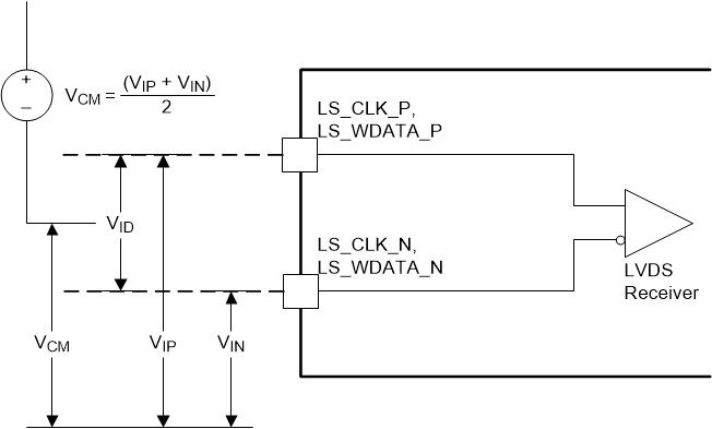 Figure 5-7 LSIF Voltage
Requirements
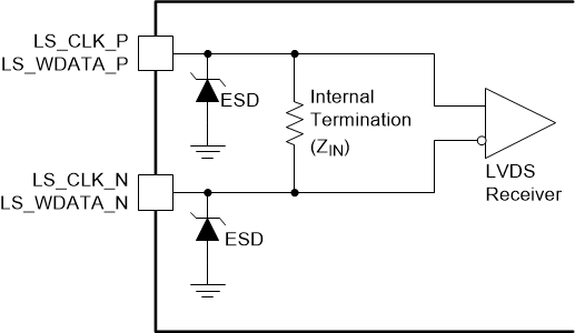 Figure 5-8 LSIF Equivalent Input
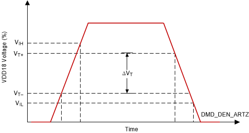 Figure 5-9 LVCMOS Input
Hysteresis
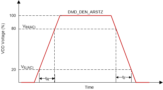 Figure 5-10 LVCMOS Rise, Fall Time Slew
Rate
Figure 5-10 LVCMOS Rise, Fall Time Slew
RateEquation 3. 

Equation 4. 

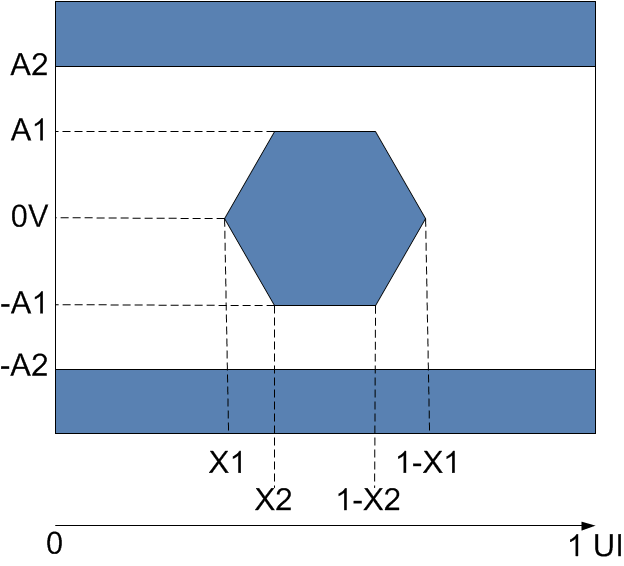 Figure 5-12 HSSI Eye Characteristics
 Figure 5-13 HSSI CLK
Characteristics
