JAJSUJ2 May 2024
ADVANCE INFORMATION
- 1
- 1 特長
- 2 アプリケーション
- 3 概要
- 4 Pin Configuration and Functions
-
5 Specifications
- 5.1 Absolute Maximum Ratings
- 5.2 Storage Conditions
- 5.3 ESD Ratings
- 5.4 Recommended Operating Conditions
- 11
- 12
- 5.5 Thermal Information
- 5.6 Electrical Characteristics
- 5.7 Switching Characteristics
- 5.8 Timing Requirements
- 5.9 System Mounting Interface Loads
- 5.10 Micromirror Array Physical Characteristics
- 5.11 Micromirror Array Optical Characteristics
- 5.12 Window Characteristics
- 5.13 Chipset Component Usage Specification
-
6 Detailed Description
- 6.1 Overview
- 6.2 Functional Block Diagram
- 6.3 Feature Description
- 6.4 Device Functional Modes
- 6.5 Optical Interface and System Image Quality Considerations
- 6.6 Micromirror Array Temperature Calculation
- 6.7 Micromirror Power Density Calculation
- 6.8 Window Aperture Illumination Overfill Calculation
- 6.9 Micromirror Landed-On/Landed-Off Duty Cycle
- 7 Application and Implementation
- 8 Power Supply Recommendations
- 9 Layout
- 10Device and Documentation Support
- 11Revision History
- 12Mechanical, Packaging, and Orderable Information
7.2.3 Application Curve
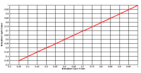
In a typical projector application, the luminous flux on the screen from the DMD depends on the optical design of the projector. The efficiency and total power of the illumination optical system and the projection optical system determine the overall light output of the projector. The DMD is inherently a linear spatial light modulator, so its efficiency just scales the light output. Figure 7-3 describes the relationship of laser input optical power to light output for a laser-phosphor illumination system, where the phosphor is not at its thermal quenching limit.
 Figure 7-3 Normalized Light Output vs. Normalized Laser Power for Laser Phosphor Illumination