JAJSOE1B April 2019 – February 2023 DLP480RE
PRODUCTION DATA
- 1 特長
- 2 アプリケーション
- 3 概要
- 4 Revision History
- 5 Pin Configuration and Functions
-
6 Specifications
- 6.1 Absolute Maximum Ratings
- 6.2 Storage Conditions
- 6.3 ESD Ratings
- 6.4 Recommended Operating Conditions
- 6.5 Thermal Information
- 6.6 Electrical Characteristics
- 6.7 Capacitance at Recommended Operating Conditions
- 6.8 Timing Requirements
- 6.9 System Mounting Interface Loads
- 6.10 Micromirror Array Physical Characteristics
- 6.11 Micromirror Array Optical Characteristics
- 6.12 Window Characteristics
- 6.13 Chipset Component Usage Specification
- 7 Detailed Description
- 8 Application and Implementation
- 9 Power Supply Recommendations
- 10Layout
- 11Device and Documentation Support
6.11 Micromirror Array Optical Characteristics
Table 6-3 Micromirror Array Optical
Characteristics
| PARAMETER | MIN | NOM | MAX | UNIT | |
|---|---|---|---|---|---|
| Mirror Tilt angle, variation device to device(1) (2) | 15.6 | 17.0 | 18.4 | degrees | |
| Number of out-of-specification micromirrors (3) | Adjacent micromirrors | 0 | micromirrors | ||
| Non-Adjacent micromirrors | 10 | ||||
| DMD Efficiency (420 nm–680 nm) |
68 |
% |
|||
(1) Limits on variability of micromirror tilt angle are critical in
the design of the accompanying optical system. Variations in tilt angle within a
device may result in apparent non-uniformities, such as line pairing and image
mottling, across the projected image. Variations in the average tilt angle
between devices may result in colorimetric and system contrast variations.
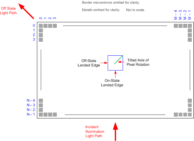
(2) See Micromirror Landed Orientation and Tilt.
(3) An out-of-specification micromirror is defined as a micromirror
that is unable to transition between the two landed states within the specified
micromirror switching time.

A. Pond of Mirrors (POM) omitted for
clarity
B. Refer to Micromirror Array
Physical Characteristics table for M, N, and P specifications.
Figure 6-9 Micromirror Landed Orientation and Tilt