JAJSHY3 September 2019 DLP5534-Q1
ADVANCE INFORMATION for pre-production products; subject to change without notice.
- 1 特長
- 2 アプリケーション
- 3 概要
- 4 改訂履歴
- 5 Pin Configuration and Functions
-
6 Specifications
- 6.1 Absolute Maximum Ratings
- 6.2 Storage Conditions
- 6.3 ESD Ratings
- 6.4 Recommended Operating Conditions
- 6.5 Thermal Information
- 6.6 Electrical Characteristics
- 6.7 Timing Requirements
- 6.8 Switching Characteristics
- 6.9 System Mounting Interface Loads
- 6.10 Physical Characteristics of the Micromirror Array
- 6.11 Micromirror Array Optical Characteristics
- 6.12 Window Characteristics
- 6.13 Chipset Component Usage Specification
- 7 Detailed Description
- 8 Application and Implementation
- 9 Power Supply Recommendations
- 10Layout
- 11デバイスおよびドキュメントのサポート
- 12メカニカル、パッケージ、および注文情報
6.8 Switching Characteristics(1)
Over operating free-air temperature range (unless otherwise noted)| PARAMETER | TEST CONDITIONS | MIN | TYP | MAX | UNIT | |
|---|---|---|---|---|---|---|
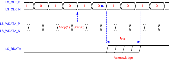
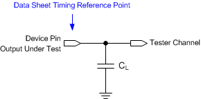
| tPD | Output propagation, clock to Q, rising edge of LS_CLK (differential clock signal) input to LS_RDATA output. See Figure 10, Figure 11 | CL = 45 pF | 15 | ns | ||
| Slew rate, LS_RDATA | 0.5 | V/ns | ||||
| Output duty cycle distortion, LS_RDATA_A and LS_RDATA_B | 40% | 60% | ||||
(1) Device electrical characteristics are over Recommended Operating Conditions unless otherwise noted.
 Figure 10. LPSDR Read Out
See Sub-LVDS Data Interface for more information.
Figure 11. Test Load Circuit for Output Propagation Measurement