JAJSHY3 September 2019 DLP5534-Q1
ADVANCE INFORMATION for pre-production products; subject to change without notice.
- 1 特長
- 2 アプリケーション
- 3 概要
- 4 改訂履歴
- 5 Pin Configuration and Functions
-
6 Specifications
- 6.1 Absolute Maximum Ratings
- 6.2 Storage Conditions
- 6.3 ESD Ratings
- 6.4 Recommended Operating Conditions
- 6.5 Thermal Information
- 6.6 Electrical Characteristics
- 6.7 Timing Requirements
- 6.8 Switching Characteristics
- 6.9 System Mounting Interface Loads
- 6.10 Physical Characteristics of the Micromirror Array
- 6.11 Micromirror Array Optical Characteristics
- 6.12 Window Characteristics
- 6.13 Chipset Component Usage Specification
- 7 Detailed Description
- 8 Application and Implementation
- 9 Power Supply Recommendations
- 10Layout
- 11デバイスおよびドキュメントのサポート
- 12メカニカル、パッケージ、および注文情報
6.10 Physical Characteristics of the Micromirror Array
| PARAMETER | VALUE | UNIT | ||||
|---|---|---|---|---|---|---|
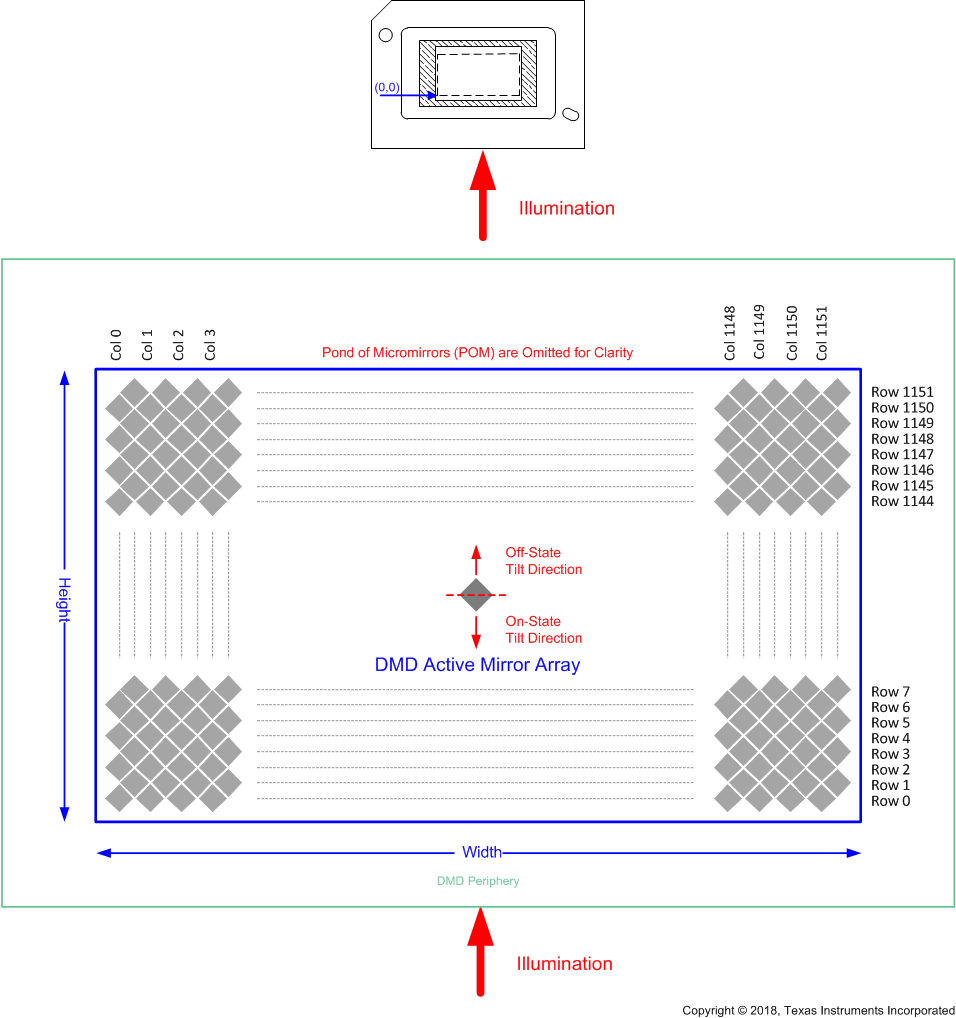
| M | Number of active columns | See Figure 13 | 1152 | micromirrors | ||
| N | Number of active rows | See Figure 13 | 1152 | micromirrors | ||
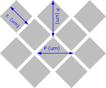
| ε | Micromirror (pixel) pitch - diagonal | See Figure 14 | 7.6 | µm | ||
| P | Micromirror (pixel) pitch - horizontal and vertical | See Figure 14 | 10.8 | µm | ||
| Micromirror active array width | P × M + P / 2; see Figure 13 | 12.447 | mm | |||
| Micromirror active array height | (P × N) / 2 + P / 2; see Figure 13 | 6.226 | mm | |||
| Micromirror active border | Pond of micromirrors (POM)(1) | 10 | micromirrors/side | |||
(1) The structure and qualities of the border around the active array includes a band of partially functional micromirrors called the POM. These micromirrors are structurally and/or electrically prevented from tilting toward the bright or ON state, but still require an electrical bias to tilt toward OFF.
 Figure 13. Micromirror Array Physical Characteristics
  Figure 14. Mirror (Pixel) Pitch