JAJSHY3 September 2019 DLP5534-Q1
ADVANCE INFORMATION for pre-production products; subject to change without notice.
- 1 特長
- 2 アプリケーション
- 3 概要
- 4 改訂履歴
- 5 Pin Configuration and Functions
-
6 Specifications
- 6.1 Absolute Maximum Ratings
- 6.2 Storage Conditions
- 6.3 ESD Ratings
- 6.4 Recommended Operating Conditions
- 6.5 Thermal Information
- 6.6 Electrical Characteristics
- 6.7 Timing Requirements
- 6.8 Switching Characteristics
- 6.9 System Mounting Interface Loads
- 6.10 Physical Characteristics of the Micromirror Array
- 6.11 Micromirror Array Optical Characteristics
- 6.12 Window Characteristics
- 6.13 Chipset Component Usage Specification
- 7 Detailed Description
- 8 Application and Implementation
- 9 Power Supply Recommendations
- 10Layout
- 11デバイスおよびドキュメントのサポート
- 12メカニカル、パッケージ、および注文情報
8.2 Typical Application
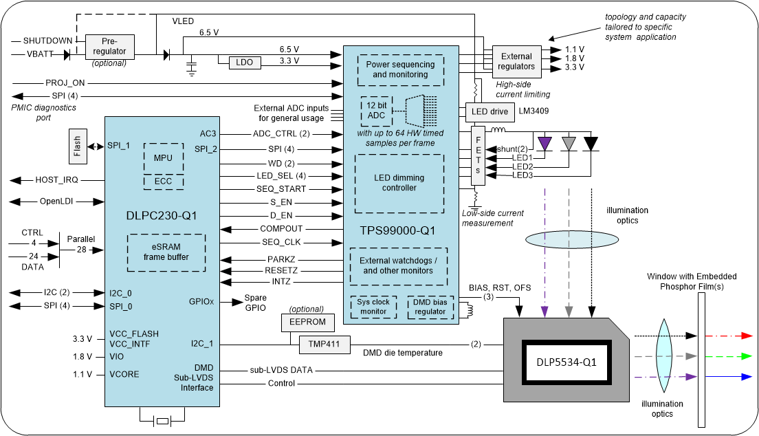
The chipset consists of three components—the DLP5534-Q1 automotive DMD, the DLPC230-Q1, and the TPS99000-Q1. The DMD is a light modulator consisting of tiny mirrors that are used to form and project images. The DLPC230-Q1 is a controller for the DMD; it formats incoming video and controls the timing of the DMD illumination sources and the DMD in order to display the incoming video. The TPS99000-Q1 is a controller for the illumination sources (e.g. LEDs or lasers) and a management IC for the entire chipset. In conjunction, the DLPC230-Q1 and the TPS99000-Q1 can also be used for system-level monitoring, diagnostics, and failure detection features. Figure 20 is a system level block diagram with these devices in the DLP head-uptransparent window display configuration and shows the primary features and functions of each device.
 Figure 20. Transparent Window Display System Block Diagram