JAJSHY3 September 2019 DLP5534-Q1
ADVANCE INFORMATION for pre-production products; subject to change without notice.
- 1 特長
- 2 アプリケーション
- 3 概要
- 4 改訂履歴
- 5 Pin Configuration and Functions
-
6 Specifications
- 6.1 Absolute Maximum Ratings
- 6.2 Storage Conditions
- 6.3 ESD Ratings
- 6.4 Recommended Operating Conditions
- 6.5 Thermal Information
- 6.6 Electrical Characteristics
- 6.7 Timing Requirements
- 6.8 Switching Characteristics
- 6.9 System Mounting Interface Loads
- 6.10 Physical Characteristics of the Micromirror Array
- 6.11 Micromirror Array Optical Characteristics
- 6.12 Window Characteristics
- 6.13 Chipset Component Usage Specification
- 7 Detailed Description
- 8 Application and Implementation
- 9 Power Supply Recommendations
- 10Layout
- 11デバイスおよびドキュメントのサポート
- 12メカニカル、パッケージ、および注文情報
9.3 Power Supply Sequencing Requirements

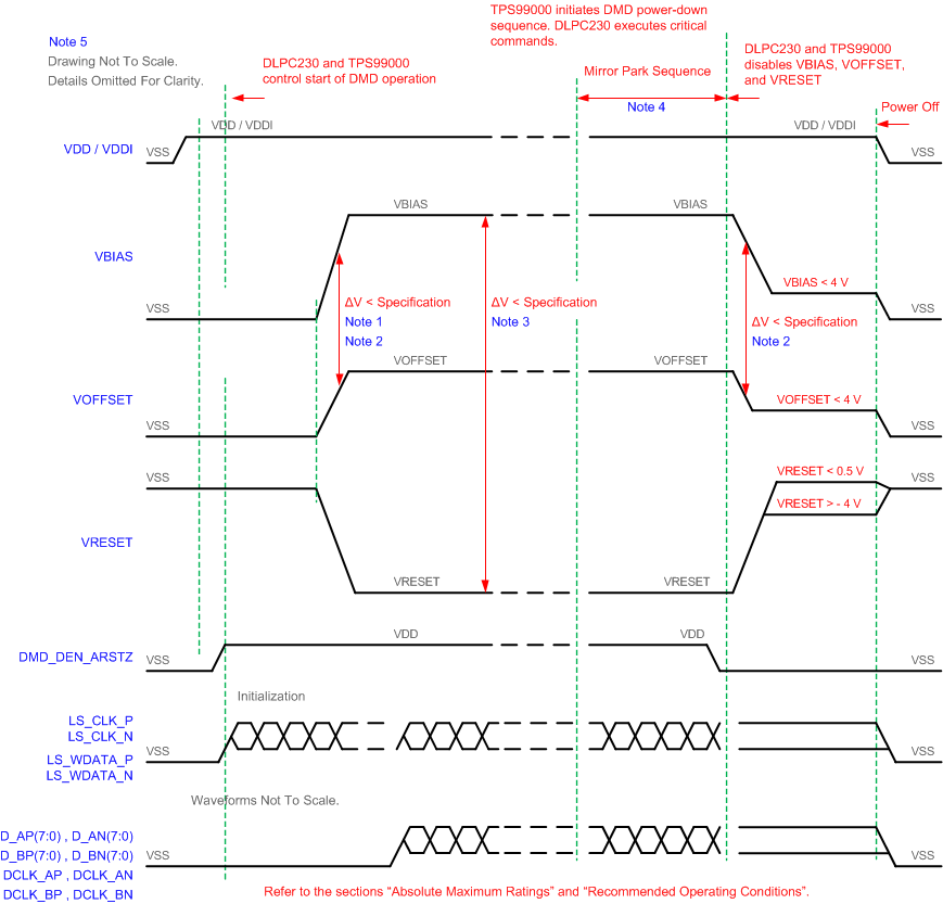
1. To prevent excess current, the supply voltage delta |VBIAS – VOFFSET| must be less than specified in the Recommended Operating Conditions. OEMs may find that the most reliable way to ensure this is to power VOFFSET prior to VBIAS during power-up and to remove VBIAS prior to VOFFSET during power-down. Also, TPS99000-Q1 is capable of managing the timing between VBIAS and VOFFSET.
2. To prevent excess current, the supply voltage delta |VBIAS – VRESET| must be less than specified than the limit shown in the Recommended Operating Conditions.
3. When system power is interrupted, the TPS9000 initiates hardware power-down that disables VBIAS, VRESET and VOFFSET after the Micromirror Park Sequence.
4. Drawing is not to scale and details are omitted for clarity.
Figure 21. Power Supply Sequencing Requirements (Power Up and Power Down)