JAJSLH9A March 2021 – May 2022 DLP650TE
PRODUCTION DATA
- 1 特長
- 2 アプリケーション
- 3 概要
- 4 Revision History
- 5 Pin Configuration and Functions
-
6 Specifications
- 6.1 Absolute Maximum Ratings
- 6.2 Storage Conditions
- 6.3 ESD Ratings
- 6.4 Recommended Operating Conditions
- 11
- 6.5 Thermal Information
- 6.6 Electrical Characteristics
- 6.7 Switching Characteristics
- 15
- 6.8 Timing Requirements
- 17
- 6.9 System Mounting Interface Loads
- 19
- 6.10 Micromirror Array Physical Characteristics
- 21
- 6.11 Micromirror Array Optical Characteristics
- 23
- 6.12 Window Characteristics
- 6.13 Chipset Component Usage Specification
- 7 Detailed Description
- 8 Application and Implementation
- 9 Power Supply Recommendations
- 10Layout
- 11Device and Documentation Support
- 12Mechanical, Packaging, and Orderable Information
10.6 Trace Length Matching Recommendations
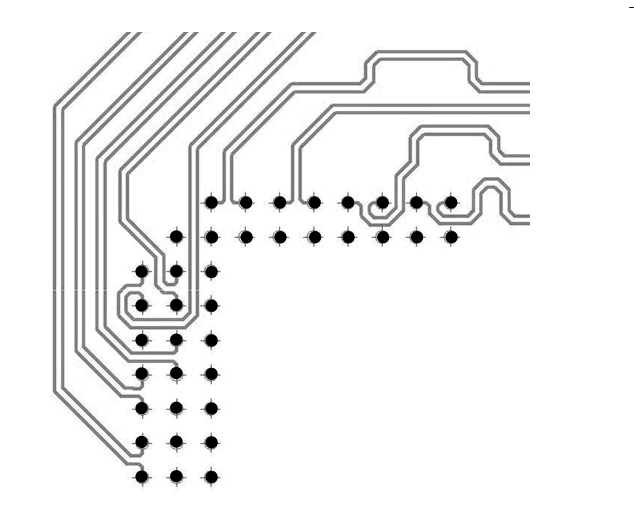
Table 10-4 and Table 10-5 describe recommended signal trace length matching requirements. Follow these guidelines to avoid routing long traces over large areas of the PCB:
- Match the trace lengths so that longer signals route in a serpentine pattern
- Minimize the number of turns.
- Ensure that the turn angles no sharper than 45 degrees.
Figure 10-1 shows an example of the HSSI signal pair routing.
Signals listed in Table 10-4 are specified for data rate operation at up to 3.2 Gbps. Minimize the layer changes for these signals. Minimize the number of vias. Avoid sharp turns and layer switching while minimizing the lengths. When layer changes are necessary, place GND vias around the signal vias to provide a signal return path. The distance from one pair of differential signals to another must be at least 2 times the distance within the pair.
| SIGNAL NAME | REFERENCE SIGNAL | ROUTING SPECIFICATION | UNIT |
|---|---|---|---|
| DMD_HSSI0_N(0...7), DMD_HSSI0_P(0...7) | DMD_HSSI0_CLK_N, DMD_HSSI_CLK_P | ±0.25 | inch |
| DMD_HSSI1_N(0...7), DMD_HSSI1_P(0...7) | DMD_HSSI0_CLK_N, DMD_HSSI_CLK_P | ±0.25 | inch |
| DMD_HSSI0_CLK_P | DMD_HSSI1_CLK_P | ±0.05 | inch |
| Intra-pair P | Intra-pair N | ±0.01 | inch |
| SIGNAL NAME | Constraints | Routing Layers |
|---|---|---|
| LS_CLK_P, LS_CLK_N LS_WDATA_P, LS_WDATA_N LS_RDATA_A | Intra-pair (P to N) Matched to 0.01 inches Signal-to-signal Matched to +/- 0.25 inches | Layers 3, 8 |
 Figure 10-1 Example HSSI PCB Routing