JAJSLH9A March   2021  – May 2022 DLP650TE

PRODUCTION DATA  

  1. 特長
  2. アプリケーション
  3. 概要
  4. Revision History
  5. Pin Configuration and Functions
  6. Specifications
    1. 6.1  Absolute Maximum Ratings
    2. 6.2  Storage Conditions
    3. 6.3  ESD Ratings
    4. 6.4  Recommended Operating Conditions
    5.     11
    6. 6.5  Thermal Information
    7. 6.6  Electrical Characteristics
    8. 6.7  Switching Characteristics
    9.     15
    10. 6.8  Timing Requirements
    11.     17
    12. 6.9  System Mounting Interface Loads
    13.     19
    14. 6.10 Micromirror Array Physical Characteristics
    15.     21
    16. 6.11 Micromirror Array Optical Characteristics
    17.     23
    18. 6.12 Window Characteristics
    19. 6.13 Chipset Component Usage Specification
  7. Detailed Description
    1. 7.1 Overview
    2. 7.2 Functional Block Diagram
    3. 7.3 Feature Description
      1. 7.3.1 Power Interface
      2. 7.3.2 Timing
    4. 7.4 Device Functional Modes
    5. 7.5 Optical Interface and System Image Quality Considerations
      1. 7.5.1 Numerical Aperture and Stray Light Control
      2. 7.5.2 Pupil Match
      3. 7.5.3 Illumination Overfill
    6. 7.6 Micromirror Array Temperature Calculation
    7. 7.7 Micromirror Landed-On/Landed-Off Duty Cycle
      1. 7.7.1 Definition of Micromirror Landed-On/Landed-Off Duty Cycle
      2. 7.7.2 Landed Duty Cycle and Useful Life of the DMD
      3. 7.7.3 Landed Duty Cycle and Operational DMD Temperature
      4. 7.7.4 Estimating the Long-Term Average Landed Duty Cycle of a Product or Application
  8. Application and Implementation
    1. 8.1 Application Information
    2. 8.2 Typical Application
      1. 8.2.1 Design Requirements
      2. 8.2.2 Detailed Design Procedure
      3. 8.2.3 Application Curve
    3. 8.3 Temperature Sensor Diode
  9. Power Supply Recommendations
    1. 9.1 Power Supply Sequence Requirements
    2. 9.2 DMD Power Supply Power-Up Procedure
    3. 9.3 DMD Power Supply Power-Down Procedure
  10. 10Layout
    1. 10.1 Layout Guidelines
    2. 10.2 Impedance Requirements
    3. 10.3 Layers
    4. 10.4 Trace Width, Spacing
    5. 10.5 Power
    6. 10.6 Trace Length Matching Recommendations
  11. 11Device and Documentation Support
    1. 11.1 Third-Party Products Disclaimer
    2. 11.2 Device Support
      1. 11.2.1 Device Nomenclature
      2. 11.2.2 Device Markings
    3. 11.3 Documentation Support
      1. 11.3.1 Related Documentation
    4. 11.4 Receiving Notification of Documentation Updates
    5. 11.5 サポート・リソース
    6. 11.6 Trademarks
    7. 11.7 Electrostatic Discharge Caution
    8. 11.8 Glossary
  12. 12Mechanical, Packaging, and Orderable Information
    1. 12.1 Package Option Addendum
      1. 12.1.1 Packaging Information

パッケージ・オプション

メカニカル・データ(パッケージ|ピン)
サーマルパッド・メカニカル・データ
発注情報

Temperature Sensor Diode

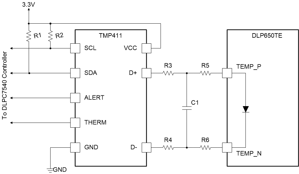
The DMD features a built-in thermal diode that measures the temperature at one corner of the die outside the micromirror array. The thermal diode can be interfaced with the TMP411 temperature sensor as shown in Figure 8-4. The software application contains functions to configure the TMP411 to read the DLP650TE DMD temperature sensor diode. This data can be leveraged by the customer to incorporate additional functionality in the overall system design such as adjusting illumination, fan speeds, and so on. All communication between the TMP411 and the DLPC7540 controller happens over the I2C interface. The TMP411 connects to the DMD via pins outlined in Table 5-1.

Leave TEMP_N and TEMP_P pins unconnected (NC) if the temp sensor is not used.
GUID-20200924-CA0I-Q4LH-8JQB-TW8DJQL8805X-low.gif
Details omitted for clarity.
See the TMP411 data sheet for system board layout recommendation.
See the TMP411 data sheet for suggested component values for R1, R2, R3, R4, and C1.
R5 = 0 Ω. R6 = 0 Ω. Place 0-Ω resistors close to the DMD package pins.
Figure 8-4 TMP411 Sample Schematic