JAJSLH9A March   2021  – May 2022 DLP650TE

PRODUCTION DATA  

  1. 特長
  2. アプリケーション
  3. 概要
  4. Revision History
  5. Pin Configuration and Functions
  6. Specifications
    1. 6.1  Absolute Maximum Ratings
    2. 6.2  Storage Conditions
    3. 6.3  ESD Ratings
    4. 6.4  Recommended Operating Conditions
    5.     11
    6. 6.5  Thermal Information
    7. 6.6  Electrical Characteristics
    8. 6.7  Switching Characteristics
    9.     15
    10. 6.8  Timing Requirements
    11.     17
    12. 6.9  System Mounting Interface Loads
    13.     19
    14. 6.10 Micromirror Array Physical Characteristics
    15.     21
    16. 6.11 Micromirror Array Optical Characteristics
    17.     23
    18. 6.12 Window Characteristics
    19. 6.13 Chipset Component Usage Specification
  7. Detailed Description
    1. 7.1 Overview
    2. 7.2 Functional Block Diagram
    3. 7.3 Feature Description
      1. 7.3.1 Power Interface
      2. 7.3.2 Timing
    4. 7.4 Device Functional Modes
    5. 7.5 Optical Interface and System Image Quality Considerations
      1. 7.5.1 Numerical Aperture and Stray Light Control
      2. 7.5.2 Pupil Match
      3. 7.5.3 Illumination Overfill
    6. 7.6 Micromirror Array Temperature Calculation
    7. 7.7 Micromirror Landed-On/Landed-Off Duty Cycle
      1. 7.7.1 Definition of Micromirror Landed-On/Landed-Off Duty Cycle
      2. 7.7.2 Landed Duty Cycle and Useful Life of the DMD
      3. 7.7.3 Landed Duty Cycle and Operational DMD Temperature
      4. 7.7.4 Estimating the Long-Term Average Landed Duty Cycle of a Product or Application
  8. Application and Implementation
    1. 8.1 Application Information
    2. 8.2 Typical Application
      1. 8.2.1 Design Requirements
      2. 8.2.2 Detailed Design Procedure
      3. 8.2.3 Application Curve
    3. 8.3 Temperature Sensor Diode
  9. Power Supply Recommendations
    1. 9.1 Power Supply Sequence Requirements
    2. 9.2 DMD Power Supply Power-Up Procedure
    3. 9.3 DMD Power Supply Power-Down Procedure
  10. 10Layout
    1. 10.1 Layout Guidelines
    2. 10.2 Impedance Requirements
    3. 10.3 Layers
    4. 10.4 Trace Width, Spacing
    5. 10.5 Power
    6. 10.6 Trace Length Matching Recommendations
  11. 11Device and Documentation Support
    1. 11.1 Third-Party Products Disclaimer
    2. 11.2 Device Support
      1. 11.2.1 Device Nomenclature
      2. 11.2.2 Device Markings
    3. 11.3 Documentation Support
      1. 11.3.1 Related Documentation
    4. 11.4 Receiving Notification of Documentation Updates
    5. 11.5 サポート・リソース
    6. 11.6 Trademarks
    7. 11.7 Electrostatic Discharge Caution
    8. 11.8 Glossary
  12. 12Mechanical, Packaging, and Orderable Information
    1. 12.1 Package Option Addendum
      1. 12.1.1 Packaging Information

パッケージ・オプション

メカニカル・データ(パッケージ|ピン)
サーマルパッド・メカニカル・データ
発注情報

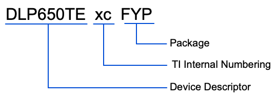
Device Nomenclature

GUID-6B5D2998-BB8A-4B14-87F5-AF018B747CB8-low.gif Figure 11-1 Part Number Description