JAJSKR6B October 2021 – April 2024 DLP800RE
PRODUCTION DATA
- 1
- 1 特長
- 2 アプリケーション
- 3 概要
- 4 Pin Configuration and Functions
-
5 Specifications
- 5.1 Absolute Maximum Ratings
- 5.2 Storage Conditions
- 5.3 ESD Ratings
- 5.4 Recommended Operating Conditions
- 11
- 5.5 Thermal Information
- 5.6 Electrical Characteristics
- 5.7 Timing Requirements
- 15
- 5.8 System Mounting Interface Loads
- 17
- 5.9 Micromirror Array Physical Characteristics
- 19
- 5.10 Micromirror Array Optical Characteristics
- 21
- 5.11 Window Characteristics
- 5.12 Chipset Component Usage Specification
-
6 Detailed Description
- 6.1 Overview
- 6.2 Functional Block Diagram
- 6.3 Feature Description
- 6.4 Device Functional Modes
- 6.5 Optical Interface and System Image Quality Considerations
- 6.6 Micromirror Array Temperature Calculation
- 6.7 Micromirror Power Density Calculation
- 6.8 Window Aperture Illumination Overfill Calculation
- 6.9 Micromirror Landed-On/Landed-Off Duty Cycle
- 7 Application and Implementation
- 8 Power Supply Recommendations
- 9 Layout
- 10Device and Documentation Support
- 11Revision History
- 12Mechanical, Packaging, and Orderable Information
6.6 Micromirror Array Temperature Calculation
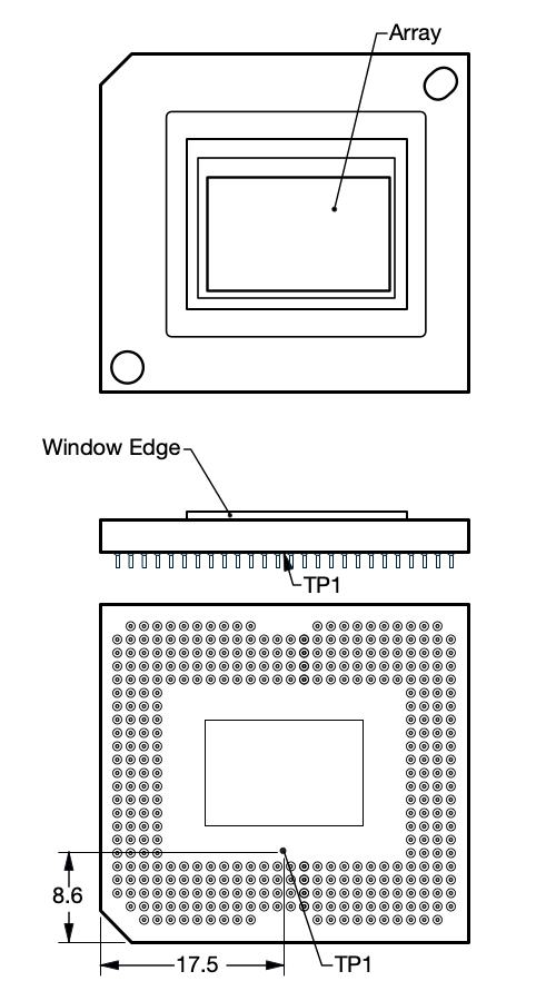
 Figure 6-1 DMD Thermal Test Point
Micromirror array temperature cannot be measured directly, therefore it must be computed analytically from a measurement point on the outside of the package, the package thermal resistance, the electrical power, and the illumination heat load. The following equations show the relationship between array temperature and the reference ceramic temperature, thermal test TP1, shown above:
where
- TARRAY = Computed array temperature (°C)
- TCERAMIC = Measured ceramic temperature (°C) (TP1 location)
- RARRAY-TO-CERAMIC = Thermal resistance of package specified in Section 5.5 from array to ceramic TP1 (°C/Watt)
- QARRAY = Total DMD power on the array (W) (electrical + absorbed)
- QELECTRICAL = Nominal electrical power (W)
- QINCIDENT = Incident illumination optical power (W)
- QILLUMINATION = (DMD average thermal absorptivity × QINCIDENT) (W)
- DMD average thermal absorptivity = 0.55
The electrical power dissipation of the DMD is variable and depends on the voltages, data rates, and operating frequencies. A nominal electrical power dissipation to use when calculating array temperature is 1.2W. The absorbed power from the illumination source is variable and depends on the operating state of the micromirrors and the intensity of the light source. The equations shown above are valid for a single chip or multichip DMD system. It assumes an illumination distribution of 83.7% on the active array, and 16.3% on the array border.
The sample calculation for a typical projection application is as follows: