JAJSKR6B October 2021 – April 2024 DLP800RE
PRODUCTION DATA
- 1
- 1 特長
- 2 アプリケーション
- 3 概要
- 4 Pin Configuration and Functions
-
5 Specifications
- 5.1 Absolute Maximum Ratings
- 5.2 Storage Conditions
- 5.3 ESD Ratings
- 5.4 Recommended Operating Conditions
- 11
- 5.5 Thermal Information
- 5.6 Electrical Characteristics
- 5.7 Timing Requirements
- 15
- 5.8 System Mounting Interface Loads
- 17
- 5.9 Micromirror Array Physical Characteristics
- 19
- 5.10 Micromirror Array Optical Characteristics
- 21
- 5.11 Window Characteristics
- 5.12 Chipset Component Usage Specification
-
6 Detailed Description
- 6.1 Overview
- 6.2 Functional Block Diagram
- 6.3 Feature Description
- 6.4 Device Functional Modes
- 6.5 Optical Interface and System Image Quality Considerations
- 6.6 Micromirror Array Temperature Calculation
- 6.7 Micromirror Power Density Calculation
- 6.8 Window Aperture Illumination Overfill Calculation
- 6.9 Micromirror Landed-On/Landed-Off Duty Cycle
- 7 Application and Implementation
- 8 Power Supply Recommendations
- 9 Layout
- 10Device and Documentation Support
- 11Revision History
- 12Mechanical, Packaging, and Orderable Information
8.3 DMD Power Supply Power-Down Procedure
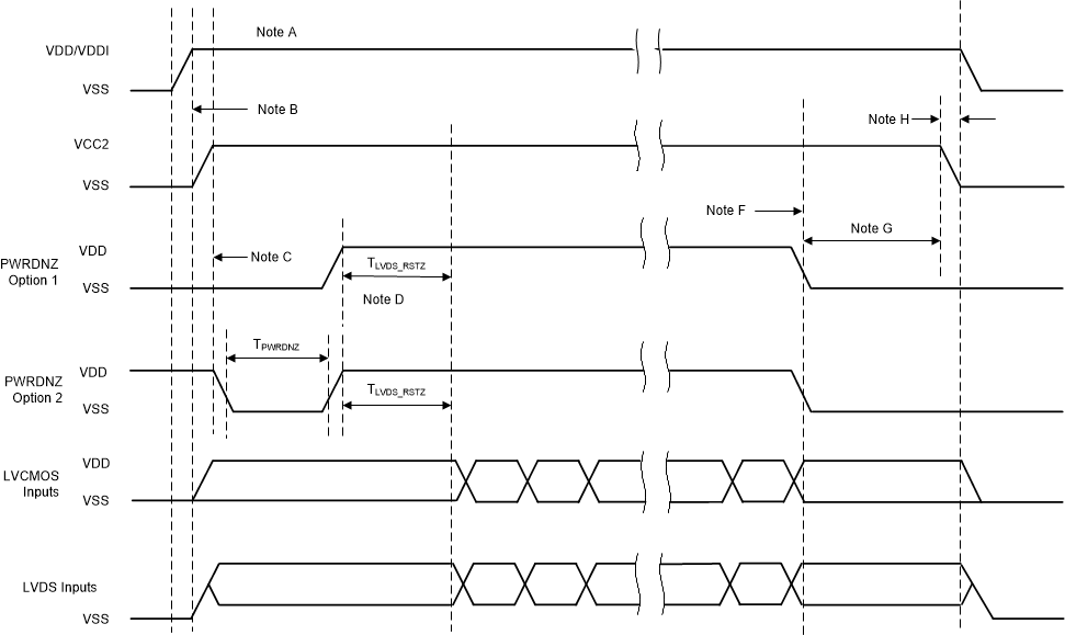
- During power-down, VDD and VDDI must be supplied until after VCC2 is discharged to within the specified limit of ground. Refer to Section 5.4.
- Power supply slew rates during power-down are flexible, provided that the transient voltage levels follow the requirements listed in Section 5.1 and in Section 5.4.
- During power-down, LVCMOS input pins must be less than specified in Section 5.4.
 Figure 8-1 DMD Power
Supply Sequencing Requirements
Figure 8-1 DMD Power
Supply Sequencing RequirementsA. See Pin
Configuration and Functions for pin functions.
B. VDD must be up
and stable prior to VCC2 powering up.
C. PWRDNZ has two
turn on options. Option 1: PWRDNZ does not go high until VDD
and VCC2 are up and stable, or Option 2: PWRDNZ must be
pulsed low for a minimum of TPWRDNZ, or 10ns
after VDD and VCC2 are up and stable.
D. There is a
minimum of TLVDS_ARSTZ, or
2μs,
wait time from PWRDNZ going high for the LVDS receiver to
recover.
E. After the DMD
micromirror park sequence is complete, the DLP controller
software initiates a hardware power-down that activates the
PWRDNZ and disables VCC2.
F. Under power-loss
conditions, where emergency DMD micromirror
park
procedures are being enacted by the DLP controller hardware,
PWRDNZ goes low.
G. VDD must remain
high until after VCC2 goes low.
H. To prevent excess
current, the supply voltage delta |VDDI – VDD| must be less
than specified limit in Section 5.4.