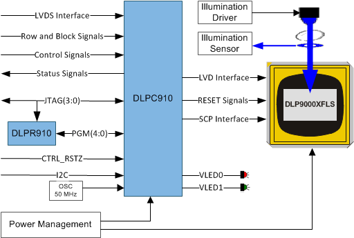
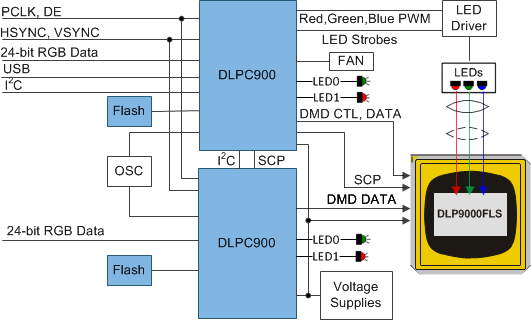
Featuring over 4 million micromirrors, the high resolution DLP9000 and DLP9000X digital micromirror devices (DMDs) are spatial light modulators (SLMs) that modulate the amplitude, direction, and/or phase of incoming light. This advanced light control technology has numerous applications in the industrial, medical, and consumer markets. The streaming nature of the DLP9000X and its DLPC910 controller enable very high speed continuous data streaming for lithographic applications. Both DMDs enable large build sizes and fine resolution for 3D printing applications. The high resolution provides the direct benefit of scanning larger objects for 3D machine vision applications.
PART NUMBER | PACKAGE | BODY SIZE (NOM) |
---|---|---|
DLP9000 | CLGA (355) | 42.20 mm x 42.20 mm x 7.00 mm |
DLP9000X |
SPACE
Changes from A Revision (October 2015) to B Revision
Changes from * Revision (September 2014) to A Revision
Reliable function and operation of the DLP9000 family requires that each DMD be used in conjunction with its specific digital controller. The DLP9000X must be driven by a single DLPC910 Controller and the DLP9000 must be driven by two DLPC900 Controllers. These dedicated chipsets provide robust, high resolution, high speed system solutions.
PIN (1) | TYPE (I/O/P) |
SIGNAL | DATA RATE (2) |
INTERNAL TERM (3) |
DESCRIPTION | TRACE (mils) (4) |
|
---|---|---|---|---|---|---|---|
NAME | NO. | ||||||
DATA BUS A | |||||||
D_AN(0) | H10 | Input | LVDS | DDR | Differential | Data, Negative | 737 |
D_AN(1) | G3 | Input | LVDS | DDR | Differential | Data, Negative | 737 |
D_AN(2) | G9 | Input | LVDS | DDR | Differential | Data, Negative | 737 |
D_AN(3) | F4 | Input | LVDS | DDR | Differential | Data, Negative | 738 |
D_AN(4) | F10 | Input | LVDS | DDR | Differential | Data, Negative | 739 |
D_AN(5) | E3 | Input | LVDS | DDR | Differential | Data, Negative | 739 |
D_AN(6) | E9 | Input | LVDS | DDR | Differential | Data, Negative | 737 |
D_AN(7) | D2 | Input | LVDS | DDR | Differential | Data, Negative | 737 |
D_AN(8) | J5 | Input | LVDS | DDR | Differential | Data, Negative | 739 |
D_AN(9) | C9 | Input | LVDS | DDR | Differential | Data, Negative | 736 |
D_AN(10) | F14 | Input | LVDS | DDR | Differential | Data, Negative | 743 |
D_AN(11) | B8 | Input | LVDS | DDR | Differential | Data, Negative | 737 |
D_AN(12) | G15 | Input | LVDS | DDR | Differential | Data, Negative | 739 |
D_AN(13) | B14 | Input | LVDS | DDR | Differential | Data, Negative | 740 |
D_AN(14) | H16 | Input | LVDS | DDR | Differential | Data, Negative | 737 |
D_AN(15) | D16 | Input | LVDS | DDR | Differential | Data, Negative | 737 |
D_AP(0) | H8 | Input | LVDS | DDR | Differential | Data, Positive | 737 |
D_AP(1) | G5 | Input | LVDS | DDR | Differential | Data, Positive | 738 |
D_AP(2) | G11 | Input | LVDS | DDR | Differential | Data, Positive | 737 |
D_AP(3) | F2 | Input | LVDS | DDR | Differential | Data, Positive | 736 |
D_AP(4) | F8 | Input | LVDS | DDR | Differential | Data, Positive | 739 |
D_AP(5) | E5 | Input | LVDS | DDR | Differential | Data, Positive | 738 |
D_AP(6) | E11 | Input | LVDS | DDR | Differential | Data, Positive | 737 |
D_AP(7) | D4 | Input | LVDS | DDR | Differential | Data, Positive | 737 |
D_AP(8) | J3 | Input | LVDS | DDR | Differential | Data, Positive | 739 |
D_AP(9) | C11 | Input | LVDS | DDR | Differential | Data, Positive | 737 |
D_AP(10) | F16 | Input | LVDS | DDR | Differential | Data, Positive | 741 |
D_AP(11) | B10 | Input | LVDS | DDR | Differential | Data, Positive | 737 |
D_AP(12) | H14 | Input | LVDS | DDR | Differential | Data, Positive | 739 |
D_AP(13) | B16 | Input | LVDS | DDR | Differential | Data, Positive | 739 |
D_AP(14) | G17 | Input | LVDS | DDR | Differential | Data, Positive | 737 |
D_AP(15) | D14 | Input | LVDS | DDR | Differential | Data, Positive | 737 |
DATA BUS B | |||||||
D_BN(0) | AD8 | Input | LVDS | DDR | Differential | Data, Negative | 739 |
D_BN(1) | AE3 | Input | LVDS | DDR | Differential | Data, Negative | 737 |
D_BN(2) | AF8 | Input | LVDS | DDR | Differential | Data, Negative | 736 |
D_BN(3) | AF2 | Input | LVDS | DDR | Differential | Data, Negative | 739 |
D_BN(4) | AG5 | Input | LVDS | DDR | Differential | Data, Negative | 737 |
D_BN(5) | AH8 | Input | LVDS | DDR | Differential | Data, Negative | 737 |
D_BN(6) | AG9 | Input | LVDS | DDR | Differential | Data, Negative | 737 |
D_BN(7) | AH2 | Input | LVDS | DDR | Differential | Data, Negative | 739 |
D_BN(8) | AL9 | Input | LVDS | DDR | Differential | Data, Negative | 737 |
D_BN(9) | AJ11 | Input | LVDS | DDR | Differential | Data, Negative | 738 |
D_BN(10) | AF14 | Input | LVDS | DDR | Differential | Data, Negative | 736 |
D_BN(11) | AE11 | Input | LVDS | DDR | Differential | Data, Negative | 737 |
D_BN(12) | AH16 | Input | LVDS | DDR | Differential | Data, Negative | 740 |
D_BN(13) | AD14 | Input | LVDS | DDR | Differential | Data, Negative | 737 |
D_BN(14) | AG17 | Input | LVDS | DDR | Differential | Data, Negative | 738 |
D_BN(15) | AD16 | Input | LVDS | DDR | Differential | Data, Negative | 738 |
D_BP(0) | AD10 | Input | LVDS | DDR | Differential | Data, Positive | 738 |
D_BP(1) | AE5 | Input | LVDS | DDR | Differential | Data, Positive | 737 |
D_BP(2) | AF10 | Input | LVDS | DDR | Differential | Data, Positive | 737 |
D_BP(3) | AF4 | Input | LVDS | DDR | Differential | Data, Positive | 738 |
D_BP(4) | AG3 | Input | LVDS | DDR | Differential | Data, Positive | 737 |
D_BP(5) | AH10 | Input | LVDS | DDR | Differential | Data, Positive | 737 |
D_BP(6) | AG11 | Input | LVDS | DDR | Differential | Data, Positive | 737 |
D_BP(7) | AH4 | Input | LVDS | DDR | Differential | Data, Positive | 740 |
D_BP(8) | AL11 | Input | LVDS | DDR | Differential | Data, Positive | 736 |
D_BP(9) | AJ9 | Input | LVDS | DDR | Differential | Data, Positive | 739 |
D_BP(10) | AF16 | Input | LVDS | DDR | Differential | Data, Positive | 737 |
D_BP(11) | AE9 | Input | LVDS | DDR | Differential | Data, Positive | 737 |
D_BP(12) | AH14 | Input | LVDS | DDR | Differential | Data, Positive | 737 |
D_BP(13) | AE15 | Input | LVDS | DDR | Differential | Data, Positive | 737 |
D_BP(14) | AG15 | Input | LVDS | DDR | Differential | Data, Positive | 740 |
D_BP(15) | AE17 | Input | LVDS | DDR | Differential | Data, Positive | 739 |
DATA BUS C | |||||||
D_CN(0) | C15 | Input | LVDS | DDR | Differential | Data, Negative | 737 |
D_CN(1) | E15 | Input | LVDS | DDR | Differential | Data, Negative | 737 |
D_CN(2) | A17 | Input | LVDS | DDR | Differential | Data, Negative | 736 |
D_CN(3) | F20 | Input | LVDS | DDR | Differential | Data, Negative | 737 |
D_CN(4) | B20 | Input | LVDS | DDR | Differential | Data, Negative | 738 |
D_CN(5) | G21 | Input | LVDS | DDR | Differential | Data, Negative | 737 |
D_CN(6) | D22 | Input | LVDS | DDR | Differential | Data, Negative | 737 |
D_CN(7) | E23 | Input | LVDS | DDR | Differential | Data, Negative | 737 |
D_CN(8) | B26 | Input | LVDS | DDR | Differential | Data, Negative | 739 |
D_CN(9) | F28 | Input | LVDS | DDR | Differential | Data, Negative | 737 |
D_CN(10) | C27 | Input | LVDS | DDR | Differential | Data, Negative | 737 |
D_CN(11) | J29 | Input | LVDS | DDR | Differential | Data, Negative | 737 |
D_CN(12) | D26 | Input | LVDS | DDR | Differential | Data, Negative | 737 |
D_CN(13) | H26 | Input | LVDS | DDR | Differential | Data, Negative | 739 |
D_CN(14) | E29 | Input | LVDS | DDR | Differential | Data, Negative | 736 |
D_CN(15) | G29 | Input | LVDS | DDR | Differential | Data, Negative | 737 |
D_CP(0) | C17 | Input | LVDS | DDR | Differential | Data, Positive | 738 |
D_CP(1) | E17 | Input | LVDS | DDR | Differential | Data, Positive | 737 |
D_CP(2) | A15 | Input | LVDS | DDR | Differential | Data, Positive | 735 |
D_CP(3) | F22 | Input | LVDS | DDR | Differential | Data, Positive | 737 |
D_CP(4) | B22 | Input | LVDS | DDR | Differential | Data, Positive | 737 |
D_CP(5) | H20 | Input | LVDS | DDR | Differential | Data, Positive | 737 |
D_CP(6) | D20 | Input | LVDS | DDR | Differential | Data, Positive | 737 |
D_CP(7) | E21 | Input | LVDS | DDR | Differential | Data, Positive | 737 |
D_CP(8) | B28 | Input | LVDS | DDR | Differential | Data, Positive | 739 |
D_CP(9) | F26 | Input | LVDS | DDR | Differential | Data, Positive | 735 |
D_CP(10) | C29 | Input | LVDS | DDR | Differential | Data, Positive | 737 |
D_CP(11) | J27 | Input | LVDS | DDR | Differential | Data, Positive | 737 |
D_CP(12) | D28 | Input | LVDS | DDR | Differential | Data, Positive | 736 |
D_CP(13) | H28 | Input | LVDS | DDR | Differential | Data, Positive | 739 |
D_CP(14) | E27 | Input | LVDS | DDR | Differential | Data, Positive | 736 |
D_CP(15) | G27 | Input | LVDS | DDR | Differential | Data, Positive | 737 |
DATA BUS D | |||||||
D_DN(0) | AJ15 | Input | LVDS | DDR | Differential | Data, Negative | 737 |
D_DN(1) | AC27 | Input | LVDS | DDR | Differential | Data, Negative | 737 |
D_DN(2) | AK16 | Input | LVDS | DDR | Differential | Data, Negative | 738 |
D_DN(3) | AE29 | Input | LVDS | DDR | Differential | Data, Negative | 738 |
D_DN(4) | AE21 | Input | LVDS | DDR | Differential | Data, Negative | 737 |
D_DN(5) | AF20 | Input | LVDS | DDR | Differential | Data, Negative | 738 |
D_DN(6) | AL15 | Input | LVDS | DDR | Differential | Data, Negative | 737 |
D_DN(7) | AG29 | Input | LVDS | DDR | Differential | Data, Negative | 738 |
D_DN(8) | AD22 | Input | LVDS | DDR | Differential | Data, Negative | 739 |
D_DN(9) | AG21 | Input | LVDS | DDR | Differential | Data, Negative | 738 |
D_DN(10) | AJ23 | Input | LVDS | DDR | Differential | Data, Negative | 736 |
D_DN(11) | AJ29 | Input | LVDS | DDR | Differential | Data, Negative | 737 |
D_DN(12) | AF28 | Input | LVDS | DDR | Differential | Data, Negative | 737 |
D_DN(13) | AK22 | Input | LVDS | DDR | Differential | Data, Negative | 741 |
D_DN(14) | AD28 | Input | LVDS | DDR | Differential | Data, Negative | 739 |
D_DN(15) | AK28 | Input | LVDS | DDR | Differential | Data, Negative | 739 |
D_DP(0) | AJ17 | Input | LVDS | DDR | Differential | Data, Positive | 737 |
D_DP(1) | AC29 | Input | LVDS | DDR | Differential | Data, Positive | 737 |
D_DP(2) | AK14 | Input | LVDS | DDR | Differential | Data, Positive | 738 |
D_DP(3) | AE27 | Input | LVDS | DDR | Differential | Data, Positive | 737 |
D_DP(4) | AD20 | Input | LVDS | DDR | Differential | Data, Positive | 737 |
D_DP(5) | AF22 | Input | LVDS | DDR | Differential | Data, Positive | 738 |
D_DP(6) | AL17 | Input | LVDS | DDR | Differential | Data, Positive | 737 |
D_DP(7) | AG27 | Input | LVDS | DDR | Differential | Data, Positive | 738 |
D_DP(8) | AE23 | Input | LVDS | DDR | Differential | Data, Positive | 739 |
D_DP(9) | AG23 | Input | LVDS | DDR | Differential | Data, Positive | 738 |
D_DP(10) | AJ21 | Input | LVDS | DDR | Differential | Data, Positive | 736 |
D_DP(11) | AJ27 | Input | LVDS | DDR | Differential | Data, Positive | 737 |
D_DP(12) | AF26 | Input | LVDS | DDR | Differential | Data, Positive | 737 |
D_DP(13) | AK20 | Input | LVDS | DDR | Differential | Data, Positive | 740 |
D_DP(14) | AD26 | Input | LVDS | DDR | Differential | Data, Positive | 739 |
D_DP(15) | AK26 | Input | LVDS | DDR | Differential | Data, Positive | 739 |
SERIAL CONTROL | |||||||
SCTRL_AN | D8 | Input | LVDS | DDR | Differential | Serial Control, Negative | 736 |
SCTRL_BN | AK8 | Input | LVDS | DDR | Differential | Serial Control, Negative | 739 |
SCTRL_CN | G23 | Input | LVDS | DDR | Differential | Serial Control, Negative | 737 |
SCTRL_DN | AH28 | Input | LVDS | DDR | Differential | Serial Control, Negative | 739 |
SCTRL_AP | D10 | Input | LVDS | DDR | Differential | Serial Control, Positive | 736 |
SCTRL_BP | AK10 | Input | LVDS | DDR | Differential | Serial Control, Positive | 739 |
SCTRL_CP | H22 | Input | LVDS | DDR | Differential | Serial Control, Positive | 739 |
SCTRL_DP | AH26 | Input | LVDS | DDR | Differential | Serial Control, Positive | 739 |
CLOCKS | |||||||
DCLK_AN | H2 | Input | LVDS | Differential | Clock, Negative | 740 | |
DCLK_BN | AJ5 | Input | LVDS | Differential | Clock, Negative | 740 | |
DCLK_CN | C23 | Input | LVDS | Differential | Clock, Negative | 736 | |
DCLK_DN | AH22 | Input | LVDS | Differential | Clock, Negative | 736 | |
DCLK_AP | H4 | Input | LVDS | Differential | Clock, Positive | 740 | |
DCLK_BP | AJ3 | Input | LVDS | Differential | Clock, Positive | 740 | |
DCLK_CP | C21 | Input | LVDS | Differential | Clock, Positive | 736 | |
DCLK_DP | AH20 | Input | LVDS | Differential | Clock, Positive | 738 | |
SERIAL COMMUNICATIONS PORT (SCP) | |||||||
SCP_DO | AC3 | Output | LVCMOS | SDR | Serial Communications Port Output | ||
SCP_DI | AD2 | Input | LVCMOS | SDR | Pull-Down | Serial Communications Port Data Input | |
SCP_CLK | AE1 | Input | LVCMOS | Pull-Down | Serial Communications Port Clock | ||
SCP_ENZ | AD4 | Input | LVCMOS | Pull-Down | Active-low Serial Communications Port Enable | ||
MICROMIRROR RESET CONTROL | |||||||
RESET_ADDR(0) | H12 | Input | LVCMOS | Pull-Down | Reset Driver Address Select | ||
RESET_ADDR(1) | C5 | Input | LVCMOS | Pull-Down | Reset Driver Address Select | ||
RESET_ADDR(2) | B6 | Input | LVCMOS | Pull-Down | Reset Driver Address Select | ||
RESET_ADDR(3) | A19 | Input | LVCMOS | Pull-Down | Reset Driver Address Select | ||
RESET_MODE(0) | J1 | Input | LVCMOS | Pull-Down | Reset Driver Mode Select | ||
RESET_MODE(1) | G1 | Input | LVCMOS | Pull-Down | Reset Driver Mode Select | ||
RESET_SEL(0) | AK4 | Input | LVCMOS | Pull-Down | Reset Driver Level Select | ||
RESET_SEL(1) | AL13 | Input | LVCMOS | Pull-Down | Reset Driver Level Select | ||
RESET_STROBE | H6 | Input | LVCMOS | Pull-Down | Reset Address, Mode, & Level latched on rising-edge | ||
ENABLES AND INTERRUPTS | |||||||
PWRDNZ | B4 | Input | LVCMOS | Active-low Device Reset | |||
RESET_OEZ | AK24 | Input | LVCMOS | Pull-Down | Active-low output enable for DMD reset driver circuits | ||
RESETZ | AL19 | Input | LVCMOS | Pull-Down | Active-low sets Reset circuits in known VOFFSET state | ||
RESET_IRQZ | C3 | Output | LVCMOS | Active-low, output interrupt to ASIC | |||
VOLTAGE REGULATOR MONITORING | |||||||
PG_BIAS | J19 | Input | LVCMOS | Pull-Up | Active-low fault from external VBIAS regulator | ||
PG_OFFSET | A13 | Input | LVCMOS | Pull-Up | Active-low fault from external VOFFSET regulator | ||
PG_RESET | AC19 | Input | LVCMOS | Pull-Up | Active-low fault from external VRESET regulator | ||
EN_BIAS | J15 | Output | LVCMOS | Active-high enable for external VBIAS regulator | |||
EN_OFFSET | H30 | Output | LVCMOS | Active-high enable for external VOFFSET regulator | |||
EN_RESET | J17 | Output | LVCMOS | Active-high enable for external VRESET regulator | |||
LEAVE PIN UNCONNECTED | |||||||
MBRST(0) | L5 | Output | Analog | Pull-Down | For proper DMD operation, do not connect | ||
MBRST(1) | M28 | Output | Analog | Pull-Down | For proper DMD operation, do not connect | ||
MBRST(2) | P4 | Output | Analog | Pull-Down | For proper DMD operation, do not connect | ||
MBRST(3) | P30 | Output | Analog | Pull-Down | For proper DMD operation, do not connect | ||
MBRST(4) | L3 | Output | Analog | Pull-Down | For proper DMD operation, do not connect | ||
MBRST(5) | P28 | Output | Analog | Pull-Down | For proper DMD operation, do not connect | ||
MBRST(6) | P2 | Output | Analog | Pull-Down | For proper DMD operation, do not connect | ||
MBRST(7) | T28 | Output | Analog | Pull-Down | For proper DMD operation, do not connect | ||
MBRST(8) | M4 | Output | Analog | Pull-Down | For proper DMD operation, do not connect | ||
MBRST(9) | L29 | Output | Analog | Pull-Down | For proper DMD operation, do not connect | ||
MBRST(10) | T4 | Output | Analog | Pull-Down | For proper DMD operation, do not connect | ||
MBRST(11) | N29 | Output | Analog | Pull-Down | For proper DMD operation, do not connect | ||
MBRST(12) | N3 | Output | Analog | Pull-Down | For proper DMD operation, do not connect | ||
MBRST(13) | L27 | Output | Analog | Pull-Down | For proper DMD operation, do not connect | ||
MBRST(14) | R3 | Output | Analog | Pull-Down | For proper DMD operation, do not connect | ||
MBRST(15) | V28 | Output | Analog | Pull-Down | For proper DMD operation, do not connect | ||
MBRST(16) | V4 | Output | Analog | Pull-Down | For proper DMD operation, do not connect | ||
MBRST(17) | R29 | Output | Analog | Pull-Down | For proper DMD operation, do not connect | ||
MBRST(18) | Y4 | Output | Analog | Pull-Down | For proper DMD operation, do not connect | ||
MBRST(19) | AA27 | Output | Analog | Pull-Down | For proper DMD operation, do not connect | ||
MBRST(20) | W3 | Output | Analog | Pull-Down | For proper DMD operation, do not connect | ||
MBRST(21) | W27 | Output | Analog | Pull-Down | For proper DMD operation, do not connect | ||
MBRST(22) | AA3 | Output | Analog | Pull-Down | For proper DMD operation, do not connect | ||
MBRST(23) | W29 | Output | Analog | Pull-Down | For proper DMD operation, do not connect | ||
MBRST(24) | U5 | Output | Analog | Pull-Down | For proper DMD operation, do not connect | ||
MBRST(25) | U29 | Output | Analog | Pull-Down | For proper DMD operation, do not connect | ||
MBRST(26) | Y2 | Output | Analog | Pull-Down | For proper DMD operation, do not connect | ||
MBRST(27) | AA29 | Output | Analog | Pull-Down | For proper DMD operation, do not connect | ||
MBRST(28) | U3 | Output | Analog | Pull-Down | For proper DMD operation, do not connect | ||
MBRST(29) | Y30 | Output | Analog | Pull-Down | For proper DMD operation, do not connect | ||
MBRST(30) | AA5 | Output | Analog | Pull-Down | For proper DMD operation, do not connect | ||
MBRST(31) | R27 | Output | Analog | Pull-Down | For proper DMD operation, do not connect | ||
LEAVE PIN UNCONNECTED | |||||||
RESERVED_PFE | J11 | Input | LVCMOS | Pull-Down | For proper DMD operation, do not connect | ||
RESERVED_TM | AC7 | Input | LVCMOS | Pull-Down | For proper DMD operation, do not connect | ||
RESERVED_XI0 | AC25 | Input | LVCMOS | Pull-Down | For proper DMD operation, do not connect | ||
RESERVED_XI1 | AC23 | Input | LVCMOS | Pull-Down | For proper DMD operation, do not connect | ||
RESERVED_XI2 | J23 | Input | LVCMOS | Pull-Down | For proper DMD operation, do not connect | ||
RESERVED_TP0 | AC9 | Input | Analog | For proper DMD operation, do not connect | |||
RESERVED_TP1 | AC11 | Input | Analog | For proper DMD operation, do not connect | |||
RESERVED_TP2 | AC13 | Input | Analog | For proper DMD operation, do not connect | |||
LEAVE PIN UNCONNECTED | |||||||
RESERVED_BA | AC15 | Output | LVCMOS | For proper DMD operation, do not connect | |||
RESERVED_BB | J13 | Output | LVCMOS | For proper DMD operation, do not connect | |||
RESERVED_BC | AC21 | Output | LVCMOS | For proper DMD operation, do not connect | |||
RESERVED_BD | J21 | Output | LVCMOS | For proper DMD operation, do not connect | |||
RESERVED_TS | AC17 | Output | LVCMOS | For proper DMD operation, do not connect | |||
LEAVE PIN UNCONNECTED | |||||||
NO CONNECT | J7 | For proper DMD operation, do not connect | |||||
NO CONNECT | J9 | For proper DMD operation, do not connect | |||||
NO CONNECT | J25 | For proper DMD operation, do not connect |
PIN | TYPE (I/O/P) |
SIGNAL | DESCRIPTION | |
---|---|---|---|---|
NAME (1) | NO. | |||
VBIAS | A3, A9, A5, A11, A7, B2 | Power | Analog | Supply voltage for positive Bias level of Micromirror reset signal. |
VOFFSET | L1, N1, R1 | Power | Analog | Supply voltage for HVCMOS logic. |
U1, W1 | Power | Analog | Supply voltage for stepped high voltage at Micromirror address electrodes. | |
AC1, AA1 | Power | Analog | Supply voltage for Offset level of MBRST(31:0). | |
VRESET | L31, N31, R31, U31, W31, AA31 | Power | Analog | Supply voltage for negative Reset level of Micromirror reset signal. |
VCC | A21, A23, A25, A27, A29, C1, C31, E31, G31, J31, K2, AC31, AE31, AG1, AG31, AJ31, AK2, AK30, AL3, AL5, AL7, AL21, AL23, AL25, AL27 | Power | Analog | Supply voltage for LVCMOS core logic. Supply voltage for normal high level at Micromirror address electrodes. |
VCCI | H18, H24, M6, M26, P6, P26, T6, T26, V6, V26, Y6, Y26, AD6, AD12, AD18, AD24 | Power | Analog | Supply voltage for LVDS receivers. |
VSS | A1, B12, B18, B24, B30, C7, C13, C19, C25, D6, D12, D18, D24, D30, E1, E7, E13, E19, E25, F6, F12, F18, F24, F30, G7, G13, G19, G25, K4, K6, K26, K28, K30, M2, M30, N5, N27, R5, T2, T30, U27, V2, V30, W5, Y28, AB2, AB4, AB6, AB26, AB28, AB30, AC5, AD30, AE7, AE13, AE19, AE25, AF6, AF12, AF18, AF24, AF30, AG7, AG13, AG19, AG25, AH6, AH12, AH18, AH24, AH30, AJ1, AJ7, AJ13, AJ19, AJ25, AK6, AK12, AK18, AL29 | Power | Analog | Device Ground. Common return for all power. |