DLPS082 February   2017 DLPA100

PRODUCTION DATA.  

  1. Features
  2. Applications
  3. Description
    1. 3.1 Typical Application Diagram
  4. Revision History
  5. Pin Configuration and Functions
    1.     Pin Functions
  6. Specifications
    1. 6.1 Absolute Maximum Ratings
    2. 6.2 Storage Conditions
    3. 6.3 ESD Ratings
    4. 6.4 Recommended Operating Conditions
    5. 6.5 Thermal Information
    6. 6.6 Electrical Characteristics
  7. Detailed Description
    1. 7.1 Overview
    2. 7.2 Functional Block Diagram
    3. 7.3 Feature Description
      1. 7.3.1  Power Up Sequencing
      2. 7.3.2  Power Down Sequencing
      3. 7.3.3  Shutdown
        1. 7.3.3.1 Thermal
      4. 7.3.4  System Reset
      5. 7.3.5  Interrupt Logic
      6. 7.3.6  Serial Communications Port
      7. 7.3.7  Switching Regulators
        1. 7.3.7.1 Output Voltage - VOUT
        2. 7.3.7.2 Adjustable Linear Regulator - VLIN1
        3. 7.3.7.3 Adjustable Linear Regulator Control - VLIN2
      8. 7.3.8  Fan Controllers
      9. 7.3.9  Color Wheel Motor Driver
        1. 7.3.9.1 Color Wheel Motor Driver Power Dissipation
      10. 7.3.10 Color Wheel Switching Regulator Supply
    4. 7.4 Device Functional Modes
  8. Application and Implementation
    1. 8.1 Application Information
    2. 8.2 Typical Application
      1. 8.2.1 Design Requirements
      2. 8.2.2 Detailed Design Procedure
      3. 8.2.3 Application Curves
  9. Power Supply Recommendations
  10. 10Layout
    1. 10.1 Layout Guidelines
    2. 10.2 Grounding Guidelines
      1. 10.2.1 Completely Isolated Ground Regions
      2. 10.2.2 Single Isolated Ground Region
      3. 10.2.3 Non-isolated Common Ground Region
    3. 10.3 Thermal Guidelines
    4. 10.4 Motor Control Guidelines
    5. 10.5 Layout Example
  11. 11Device and Documentation Support
    1. 11.1 Device Markings
    2. 11.2 Documentation Support
      1. 11.2.1 Related Documentation
    3. 11.3 Community Resources
    4. 11.4 Trademarks
    5. 11.5 Electrostatic Discharge Caution
    6. 11.6 Glossary
  12. 12Mechanical, Packaging, and Orderable Information
    1. 12.1 Package Option Addendum
      1. 12.1.1 Packaging Information

パッケージ・オプション

メカニカル・データ(パッケージ|ピン)
  • DLP|48
サーマルパッド・メカニカル・データ

Power Up Sequencing

Once the VBB voltage reaches the VBBuvsd threshold (specification defined in Shutdown), the VCORE channel soft-starts within a period of 5 ms typical (tss). Once this period is completed and the VCOREuvlo has been reached, the V3P3 and V2P5 rails soft-start, ramping up ratiometrically. Once each of the three rails are above their respective undervoltage lockout levels (VCOREuvlo, V3P3uvlo, V2P5uvlo), the POSENSE flag will go high after a period of 150 ms typical (Tpor) and also, the VLIN1, VLIN2, V5 and VM rails soft-start, ramping up ratiometrically. Note that VLIN1, VLIN2, V5 and VM can be individually disabled via the serial port, although VLIN1 and VLIN2 require V5 to be present.

The PWRGOOD flag will go high once the POSENSE is high and the VBB voltage is above the undervoltage lockout threshold VBBuvlo.
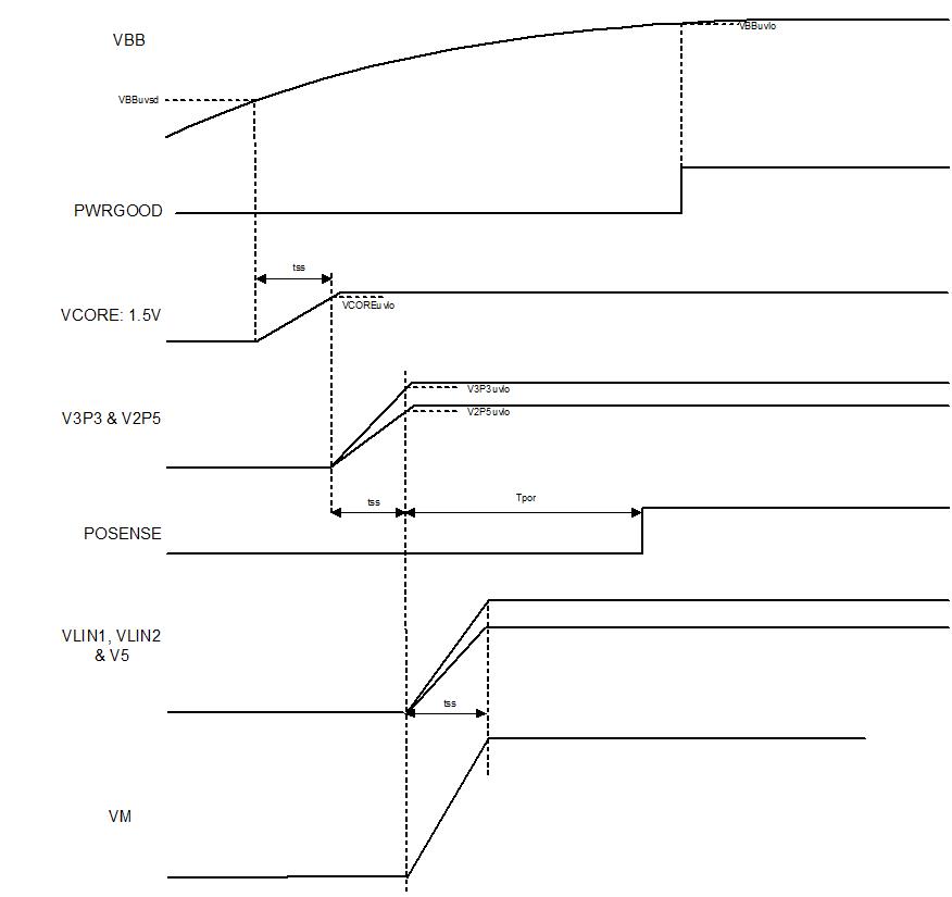
DLPA100 DLPA100_powerup_sequencing.jpgFigure 1. Power Up Sequencing Timing Diagram