JAJSF34B November 2017 – May 2022 DLPC120-Q1
PRODUCTION DATA
- 1 特長
- 2 アプリケーション
- 3 概要
- 4 Revision History
- 5 Pin Configuration and Functions
-
6 Specifications
- 6.1 Absolute Maximum Ratings
- 6.2 ESD Ratings
- 6.3 Recommended Operating Conditions
- 6.4 Thermal Information
- 6.5 Electrical Characteristics
- 6.6 Electrical Characteristics for I/O
- 6.7 Power Supply and Reset Timing Requirements
- 6.8 Reference Clock PLL Timing Requirements
- 6.9 Parallel Interface General Timing Requirements
- 6.10 Parallel Interface Frame Timing Requirements
- 6.11 Flash Memory Interface Timing Requirements
- 6.12 DMD Interface Timing Requirements
- 6.13 JTAG Interface Timing Requirements
- 6.14 I2C Interface Timing Requirements
- 7 Parameter Measurement Information
- 8 Detailed Description
- 9 Application and Implementation
- 10Power Supply Recommendations
- 11Layout
- 12Device and Documentation Support
- 13Mechanical, Packaging, and Orderable Information
パッケージ・オプション
デバイスごとのパッケージ図は、PDF版データシートをご参照ください。
メカニカル・データ(パッケージ|ピン)
- ZXS|216
サーマルパッド・メカニカル・データ
発注情報
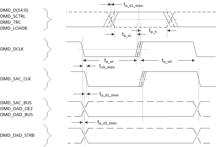
6.12 DMD Interface Timing Requirements
| MIN | NOM | MAX | UNIT | |||
|---|---|---|---|---|---|---|
| ƒclock | Clock frequency, DMD_DCLK and DMD_SAC_CLK(1) | 75.00 | 78.00 | 80.00 | MHz | |
| tp_clkper | Clock period, DMD_DCLK and DMD_SAC_CLK | 50% reference points | 12.5 | 15.0 | ns | |
| tp_clkjit | Clock jitter, DMD_DCLK and DMD_SAC_CLK | Maximum fclock | 200 | ps | ||
| tp_wh | Pulse width high, DMD_DCLK and DMD_SAC_CLK | 50% reference points | 6.2 | ns | ||
| tp_wl | Pulse width low, DMD_DCLK and DMD_SAC_CLK | 50% reference points | 6.2 | ns | ||
| tt | Transition time, all signals | 20% to 80% reference points | 0.5 | 1.5 | ns | |
| tp_su | Output setup time – DMD_D(14:0), DMD_SCTRL, DMD_LOADB and DMD_TRC relative to both rising and falling edges of DMD_DCLK(2) | 50% reference points | 1.5 | ns | ||
| tp_h | Output hold time – DMD_D(14:0), DMD_SCTRL, DMD_LOADB and DMD_TRC signals relative to both rising and falling edges of DMD_DCLK(2) | 50% reference points | 1.5 | ns | ||
| tp_d1_skew | DMD data skew – DMD_D(14:0), DMD_SCTRL, DMD_LOADB and DMD_TRC signals relative to each other | 50% reference points | 0.20 | ns | ||
| tp_d2_skew | DAD/ SAC data skew - DMD_SAC_BUS, DMD_DAD_OEZ and DMD_DAD_BUS signals relative to DMD_SAC_CLK | 50% reference points | 1.65 | ns | ||
| tp_d3_skew | DMD_DAD_STRB signal relative to DMD_DCLK | 50% reference points | 1.65 | ns | ||
| tp_clk_skew | Clock skew – DMD_DCLK and DMD_SAC_CLK relative to each other | 50% reference points | 0.25 | ns | ||
(1) This range includes the 200 PPM of the external oscillator.
(2) Output setup and hold numbers already account for ASIC clock jitter. Only routing skew and DMD setup/ hold need be considered in system timing analysis.
 Figure 6-6 DMD Interface Timing