JAJSF34B November 2017 – May 2022 DLPC120-Q1
PRODUCTION DATA
- 1 特長
- 2 アプリケーション
- 3 概要
- 4 Revision History
- 5 Pin Configuration and Functions
-
6 Specifications
- 6.1 Absolute Maximum Ratings
- 6.2 ESD Ratings
- 6.3 Recommended Operating Conditions
- 6.4 Thermal Information
- 6.5 Electrical Characteristics
- 6.6 Electrical Characteristics for I/O
- 6.7 Power Supply and Reset Timing Requirements
- 6.8 Reference Clock PLL Timing Requirements
- 6.9 Parallel Interface General Timing Requirements
- 6.10 Parallel Interface Frame Timing Requirements
- 6.11 Flash Memory Interface Timing Requirements
- 6.12 DMD Interface Timing Requirements
- 6.13 JTAG Interface Timing Requirements
- 6.14 I2C Interface Timing Requirements
- 7 Parameter Measurement Information
- 8 Detailed Description
- 9 Application and Implementation
- 10Power Supply Recommendations
- 11Layout
- 12Device and Documentation Support
- 13Mechanical, Packaging, and Orderable Information
パッケージ・オプション
デバイスごとのパッケージ図は、PDF版データシートをご参照ください。
メカニカル・データ(パッケージ|ピン)
- ZXS|216
サーマルパッド・メカニカル・データ
発注情報
5 Pin Configuration and Functions
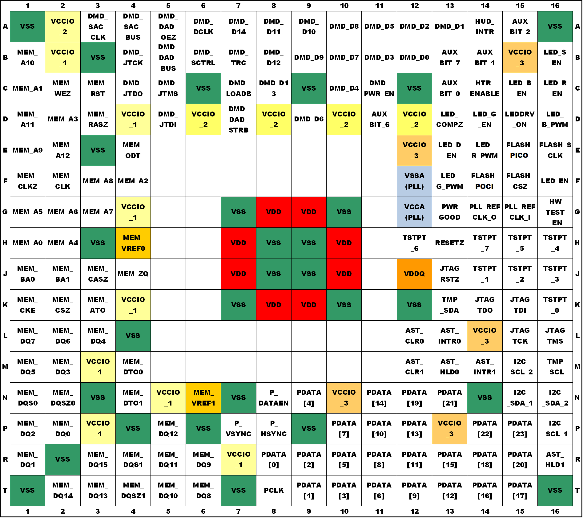
 Figure 5-1 ZXS Package216-Pin BGATop View
Table 5-1 DLPC120-Q1 Device Initialization and Programming Pin Descriptions
| PIN | I/O | I/O | CLOCK | ||
|---|---|---|---|---|---|
| NAME | NO. | POWER | TYPE | SYSTEM | DESCRIPTION |
| RESETZ | H13 | 3.30 V | I2 | Async | Functional Reset (Active Low). Resets internal logic and causes PLL startup and PLL locking. Assertion is required after power supplies are within limits. See Section 6.7 for timing requirements. |
| PWRGOOD | G13 | I2 | Async | System Power Good indicator. Should be held low until all DLPC120-Q1 power has been within operating limits. See Section 6.7 for timing requirements. Must be set high to enable normal operation. When set low, the DLPC120-Q1 begins the parking routine for the DMD. Together with pin E14 (LED_R_PWM / PWRGOOD_CNTRL), this signal is critical for DLP30xx-Q1 parking as part of the Pre-Conditioning Sequence and subsequent un-parking. See DLPC120-Q1 Programmer's Guide for implementation details. | |
| PLL_REFCLK_I | G15 | I2 | N/A | Reference Clock Input (16 MHz). Can be driven by crystal across this pin and PLL_REFCLK_O or by external oscillator. See Section 6.7 for timing requirements. | |
| PLL_REFCLK_O | G14 | O6 | N/A | Crystal output. Used with PLL_REFCLK_I. | |
| HUD_INTR | A14 | O6 | N/A | Interrupt signal. This active high signal indicates one of the interrupt sources in the controller has been triggered. | |
| IIC_SCL_1 | P16 | B8 | N/A | I2C Clock for Device configuration and control. Requires external pull-up. Port 1 peripheral command/control interface. | |
| IIC_SDA_1 | N15 | B8 | N/A | I2C Data for Device configuration and control. Requires external pull-up. Port 1 peripheral command/control interface. | |
| IIC_SCL_2 | M15 | B8 | N/A | I2C Clock Debug Port. Requires external pull-up. Port 2 peripheral command/control interface. | |
| IIC_SDA_2 | N16 | B8 | N/A | I2C Data Debug Port. Requires external pull-up. Port 2 peripheral command/control interface. | |
| FLASH_POCI | F14 | I2 | FLASH_SCLK | Serial Data input from the external SPI Flash device. This provides device logical programming data as well as functional configuration parameter data. | |
| FLASH_CSZ | F15 | O6 | FLASH_SCLK | Chip Select output for the external SPI Flash device. Active low. | |
| FLASH_SCLK | E16 | O6 | N/A | Clock for the external SPI Flash device. | |
| FLASH_PICO | E15 | O6 | FLASH_SCLK | Serial Data output to the external SPI Flash device. This pin sends address and control information as well as data when programming. | |