JAJSJA1E August 2020 – August 2024 DLPC230S-Q1 , DLPC231S-Q1
PRODUCTION DATA
- 1
- 1 特長
- 2 アプリケーション
- 3 概要
- 4 Pin Configuration and Functions
-
5 Specifications
- 5.1 Absolute Maximum Ratings
- 5.2 ESD Ratings
- 5.3 Recommended Operating Conditions
- 5.4 Thermal Information
- 5.5 Electrical Characteristics
- 5.6 Electrical Characteristics for Fixed Voltage I/O
- 5.7 DMD High-Speed SubLVDS Electrical Characteristics
- 5.8 DMD Low-Speed SubLVDS Electrical Characteristics
- 5.9 OpenLDI LVDS Electrical Characteristics
- 5.10 Power Dissipation Characterisics
- 5.11 System Oscillators Timing Requirements
- 5.12 Power Supply and Reset Timing Requirements
- 5.13 Parallel Interface General Timing Requirements
- 5.14 OpenLDI Interface General Timing Requirements
- 5.15 Parallel/OpenLDI Interface Frame Timing Requirements
- 5.16 Host/Diagnostic Port SPI Interface Timing Requirements
- 5.17 Host/Diagnostic Port I2C Interface Timing Requirements
- 5.18 Flash Interface Timing Requirements
- 5.19 TPS99000S-Q1 SPI Interface Timing Requirements
- 5.20 TPS99000S-Q1 AD3 Interface Timing Requirements
- 5.21 DLPC23xS-Q1 I2C Port Interface Timing Requirements
- 5.22 Chipset Component Usage Specification
- 6 Parameter Measurement Information
-
7 Detailed Description
- 7.1 Overview
- 7.2 Functional Block Diagram
- 7.3
Feature Description
- 7.3.1 Parallel Interface
- 7.3.2 OpenLDI Interface
- 7.3.3 DMD (SubLVDS) Interface
- 7.3.4 Serial Flash Interface
- 7.3.5 Serial Flash Programming
- 7.3.6 Host Command and Diagnostic Processor Interfaces
- 7.3.7 GPIO Supported Functionality
- 7.3.8 Built-In Self Test (BIST)
- 7.3.9 EEPROMs
- 7.3.10 Temperature Sensor
- 7.3.11 Debug Support
- 7.4 Device Functional Modes
-
8 Application and Implementation
- 8.1 Application Information
- 8.2 Typical Application
- 8.3 Power Supply Recommendations
- 8.4
Layout
- 8.4.1
Layout Guidelines
- 8.4.1.1 PCB Layout Guidelines for Internal ASIC PLL Power
- 8.4.1.2 DLPC23xS-Q1 Reference Clock
- 8.4.1.3 DMD Interface Layout Considerations
- 8.4.1.4 General PCB Recommendations
- 8.4.1.5 General Handling Guidelines for Unused CMOS-Type Pins
- 8.4.1.6 Maximum Pin-to-Pin, PCB Interconnects Etch Lengths
- 8.4.1.7 Number of Layer Changes
- 8.4.1.8 Stubs
- 8.4.1.9 Terminations
- 8.4.1.10 Routing Vias
- 8.4.2 Thermal Considerations
- 8.4.1
Layout Guidelines
- 9 Device and Documentation Support
- 10Revision History
- 11Mechanical, Packaging, and Orderable Information
パッケージ・オプション
デバイスごとのパッケージ図は、PDF版データシートをご参照ください。
メカニカル・データ(パッケージ|ピン)
- ZEK|324
サーマルパッド・メカニカル・データ
発注情報
5.18 Flash Interface Timing Requirements
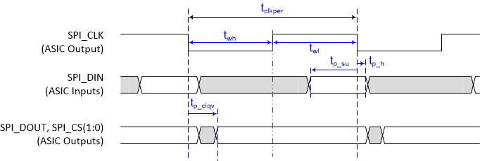
The DLPC23xS-Q1 ASIC flash memory interface consists of an SPI serial interface. See Section 7.3.4.
| (1) | MIN | MAX | UNIT | ||
|---|---|---|---|---|---|
| fclock | Clock frequency, FLSH_SPI_CLK | When VCC3IO_FLSH = 3.3VDC | 9.998 | 50.01(2) | MHz |
| tp_clkper | Clock period, FLSH_SPI_CLK (50% reference points) | When VCC3IO_FLSH = 3.3VDC | 20.0 | 100 | ns |
| tp_wh | Pulse duration low, FLSH_SPI_CLK (50% reference points) | When VCC3IO_FLSH = 3.3VDC | 9 | ns | |
| tp_wl | Pulse duration high, FLSH_SPI_CLK (50% reference points) | When VCC3IO_FLSH = 3.3VDC | 9 | ns | |
| tt | Transition time – all input signals | 20% to 80% reference points | 6 | ns | |
| tp_su | Setup time – FLSH_SPI_DIO[3:0] valid before FLSH_SPI_CLK falling edge (50% reference points) | When VCC3IO_FLSH = 3.3VDC | 7.0 | ns | |
| tp_h | Hold time – FLSH_SPI_DIO[3:0] valid after FLSH_SPI_CLK falling edge | 50% reference points | 0.0 | ns | |
| tp_clqv | FLSH_SPI_DIO[3:0] output delay valid time (with respect to falling edge of FLSH_SPI_CLK or falling edge of FLSH_SPI_CSZ) | When VCC3IO_FLSH = 3.3VDC | –3.0 | 3.0 | ns |
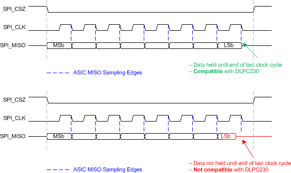
(1) The DLPC23xS-Q1 communicates with flash devices using a slight variant of SPI Transfer Mode 0 (that is, clock polarity = 0, clock phase = 0). Instead of capturing MISO data on the clock edge opposite from that used to transmit MOSI data, the DLPC23xS-Q1 captures MISO data on the same clock edge used to transmit the next MOSI data. As such, the DLPC23xS-Q1 Flash SPI interface requires that MISO data from the flash device remain active until the end of the full clock cycle to allow the last data bit to be captured. This is shown in Figure 5-8.
(2) The actual maximum clock rate driven from the DLPC23xS-Q1 can be slightly less than this value.
 Figure 5-7 Flash Interface Timing
 Figure 5-8 Flash Interface Data Capture Requirements