JAJSF42C April   2018  – December 2020 DLPC3478

PRODUCTION DATA  

  1. 特長
  2. アプリケーション
  3. 概要
  4. Revision History
  5. Pin Configuration and Functions
  6. Specifications
    1. 6.1  Absolute Maximum Ratings
    2. 6.2  ESD Ratings
    3. 6.3  Recommended Operating Conditions
    4. 6.4  Thermal Information
    5. 6.5  Power Electrical Characteristics
    6. 6.6  Pin Electrical Characteristics
    7. 6.7  Internal Pullup and Pulldown Electrical Characteristics
    8. 6.8  DMD Sub-LVDS Interface Electrical Characteristics
    9. 6.9  DMD Low-Speed Interface Electrical Characteristics
    10. 6.10 System Oscillator Timing Requirements
    11. 6.11 Power Supply and Reset Timing Requirements
    12. 6.12 Parallel Interface Frame Timing Requirements
    13. 6.13 Parallel Interface General Timing Requirements
    14. 6.14 BT656 Interface General Timing Requirements
    15. 6.15 Flash Interface Timing Requirements
    16. 6.16 Other Timing Requirements
    17. 6.17 DMD Sub-LVDS Interface Switching Characteristics
    18. 6.18 DMD Parking Switching Characteristics
    19. 6.19 Chipset Component Usage Specification
  7. Detailed Description
    1. 7.1 Overview
    2. 7.2 Functional Block Diagram
    3. 7.3 Feature Description
      1. 7.3.1  Input Source
        1. 7.3.1.1 Supported Resolution and Frame Rates
        2. 7.3.1.2 3D Display
        3. 7.3.1.3 Parallel Interface
          1. 7.3.1.3.1 PDATA Bus – Parallel Interface Bit Mapping Modes
      2. 7.3.2  Pattern Display
        1. 7.3.2.1 External Pattern Mode
          1. 7.3.2.1.1 8-bit Monochrome Patterns
          2. 7.3.2.1.2 1-Bit Monochrome Patterns
        2. 7.3.2.2 Internal Pattern Mode
          1. 7.3.2.2.1 Free Running Mode
          2. 7.3.2.2.2 Trigger In Mode
      3. 7.3.3  Device Startup
      4. 7.3.4  SPI Flash
        1. 7.3.4.1 SPI Flash Interface
        2. 7.3.4.2 SPI Flash Programming
      5. 7.3.5  I2C Interface
      6. 7.3.6  Content Adaptive Illumination Control (CAIC)
      7. 7.3.7  Local Area Brightness Boost (LABB)
      8. 7.3.8  3D Glasses Operation
      9. 7.3.9  Test Point Support
      10. 7.3.10 DMD Interface
        1. 7.3.10.1 Sub-LVDS (HS) Interface
    4. 7.4 Device Functional Modes
    5. 7.5 Programming
  8. Application and Implementation
    1. 8.1 Application Information
    2. 8.2 Typical Application
      1. 8.2.1 Pattern projector for 3D depth scanning
        1. 8.2.1.1 Design Requirements
        2. 8.2.1.2 Detailed Design Procedure
        3. 8.2.1.3 Application Curve
      2. 8.2.2 3D Depth Scanner Using Internal Pattern Streaming Mode
        1. 8.2.2.1 Design Requirements
        2. 8.2.2.2 Detailed Design Procedure
        3. 8.2.2.3 Application Curve
  9. Power Supply Recommendations
    1. 9.1 PLL Design Considerations
    2. 9.2 System Power-Up and Power-Down Sequence
    3. 9.3 Power-Up Initialization Sequence
    4. 9.4 DMD Fast Park Control (PARKZ)
    5. 9.5 Hot Plug I/O Usage
  10. 10Layout
    1. 10.1 Layout Guidelines
      1. 10.1.1 PLL Power Layout
      2. 10.1.2 Reference Clock Layout
        1. 10.1.2.1 Recommended Crystal Oscillator Configuration
      3. 10.1.3 Unused Pins
      4. 10.1.4 DMD Control and Sub-LVDS Signals
      5. 10.1.5 Layer Changes
      6. 10.1.6 Stubs
      7. 10.1.7 Terminations
      8. 10.1.8 Routing Vias
      9. 10.1.9 Thermal Considerations
    2. 10.2 Layout Example
  11. 11Device and Documentation Support
    1. 11.1 Device Support
      1. 11.1.1 Third-Party Products Disclaimer
      2. 11.1.2 Device Nomenclature
        1. 11.1.2.1 Device Markings
      3. 11.1.3 Video Timing Parameter Definitions
    2. 11.2 Documentation Support
      1. 11.2.1 Related Documentation
    3. 11.3 ドキュメントの更新通知を受け取る方法
    4. 11.4 サポート・リソース
    5. 11.5 Trademarks
    6. 11.6 静電気放電に関する注意事項
    7. 11.7 用語集
  12. 12Mechanical, Packaging, and Orderable Information

パッケージ・オプション

メカニカル・データ(パッケージ|ピン)
サーマルパッド・メカニカル・データ
発注情報

3D Display

For 3D sources on the video input interface, images must be frame sequential (L, R, L, ...) when input to the DLPC34xx controller. Any processing required to unpack 3D images and to convert them to frame sequential input must be done by external electronics prior to inputting the images to the controller. Each 3D source frame input must contain a single eye frame of data, separated by a VSYNC, where an eye frame contains image data for a single left or right eye. The signal 3DR input to the controller indicates whether the input frame is for the left eye or right eye.

Each DMD frame is displayed at the same rate as the input interface frame rate. Figure 7-1 below shows the typical timing for a 50-Hz or 60-Hz 3D HDMI source frame, the input interface of the DLPC34xx controller, and the DMD. In general, video frames sent over the HDMI interface pack both the left and right content into the same video frame. GPIO_04 is optionally sent to a transmitter on the system PCB for wirelessly transmitting a synchronization signal to 3D glasses (usually an IR sync signal). The glasses are then in phase with the DMD images displayed. Alternately, the 3D Glasses Operation section shows how DLP link pulses can be used instead.
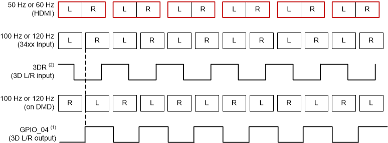
(1) Left = 1, Right = 0
(2) 3DR must toggle at least 1 ms before VSYNC
Figure 7-1 3D Display Left and Right Frame Timing