JAJSH15H October 2014 – June 2024 DLPC900
PRODUCTION DATA
- 1
- 1 特長
- 2 アプリケーション
- 3 概要
- 4 Pin Configuration and Functions
-
5 Specifications
- 5.1 Absolute Maximum Ratings
- 5.2 ESD Ratings
- 5.3 Recommended Operating Conditions
- 5.4 Thermal Information
- 5.5 Electrical Characteristics
- 5.6 System Oscillators Timing Requirements #GUID-909D0FD3-84C7-4481-924A-4FDE7EB548A1/DLPS0373944
- 5.7 Power-Up and Power-Down Timing Requirements
- 5.8 JTAG Interface: I/O Boundary Scan Application Timing Requirements
- 5.9 JTAG Interface: I/O Boundary Scan Application Switching Characteristics
- 5.10 Programmable Output Clocks Switching Characteristics
- 5.11 Port 1 and 2 Input Pixel Interface Timing Requirements
- 5.12 Two Pixels Per Clock (48-Bit Bus) Timing Requirements
- 5.13 Synchronous Serial Port (SSP) Switching Characteristics
- 5.14 DMD Interface Switching Characteristics
- 5.15 DMD LVDS Interface Switching Characteristics
- 5.16 Source Input Blanking Requirements
-
6 Detailed Description
- 6.1 Overview
- 6.2 Functional Block Diagram
- 6.3
Feature Description
- 6.3.1 DMD Configurations
- 6.3.2 Video Timing Input Blanking Specification
- 6.3.3 Board-Level Test Support
- 6.3.4 Two Controller Considerations
- 6.3.5 Memory Design Considerations
- 6.4 Device Functional Modes
-
7 Application and Implementation
- 7.1 Application Information
- 7.2
Typical Applications
- 7.2.1 Typical Two Controller Chipset
- 7.2.2 Typical Single Controller Chipset
- 8 Power Supply Recommendations
-
9 Layout
- 9.1
Layout Guidelines
- 9.1.1 General PCB Recommendations
- 9.1.2 PCB Layout Guidelines for Internal Controller PLL Power
- 9.1.3 PCB Layout Guidelines for Quality Video Performance
- 9.1.4 Recommended MOSC Crystal Oscillator Configuration
- 9.1.5 Spread Spectrum Clock Generator Support
- 9.1.6 GPIO Interface
- 9.1.7 General Handling Guidelines for Unused CMOS-Type Pins
- 9.1.8 DMD Interface Considerations
- 9.1.9 PCB Design Standards
- 9.1.10 Signal Layers
- 9.1.11 Trace Widths and Minimum Spacing
- 9.1.12 Trace Impedance and Routing Priority
- 9.1.13 Power and Ground Planes
- 9.1.14 Power Vias
- 9.1.15 Decoupling
- 9.1.16 Fiducials
- 9.2 Layout Example
- 9.3 Thermal Considerations
- 9.1
Layout Guidelines
- 10Device and Documentation Support
- 11Revision History
- 12Mechanical, Packaging, and Orderable Information
9.2 Layout Example
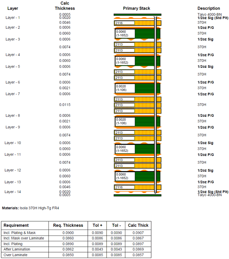
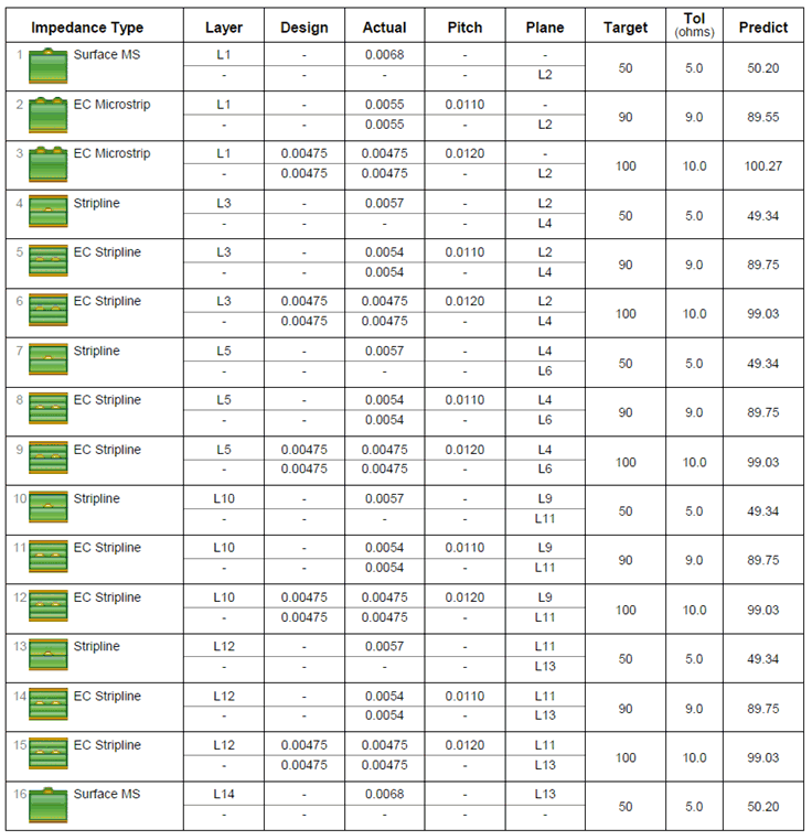
The DLP® LightCrafter™ Dual DLPC900 Evaluation Module (EVM) PCB is targeted at 14 layers with layer stack up shown in Figure 9-7. The PCB layer stack can vary depending on the system design. However, careful attention is required to meet design considerations. Layers 1 and 14 consist of the component layers. Layers 2, 4, 6, 9, 11, and 13 consist of solid ground planes. Layers 7 and 8 consist of solid power planes. Layers 1, 3, 5, 10, 12, and 14 are used as the primary routing layers. Routing on external layers must be less than 0.25 inches for priority one and two signals. Refer to the Table 9-9 for signal priority groups. Board material must be FR-370HR or similar. PCB must be designed for lead-free assembly with the stack-up geometry shown in Figure 9-7 and Figure 9-8.
 Figure 9-7 Board Layer Stack
 Figure 9-8 Board Trace Geometry
Refer to Section 9.2 for a complete set of documentation for the DLP® LightCrafter™ Dual DLPC900 Evaluation Module (EVM) reference design.