JAJST20 March 2024 DLPC964
PRODUCTION DATA
- 1
- 1 特長
- 2 アプリケーション
- 3 概要
- 4 Pin Configuration and Functions
- 5 Specifications
-
6 Detailed Description
- 6.1 Overview
- 6.2 Functional Block Diagram
- 6.3 Feature Description
- 6.4
Device Functional
Modes
- 6.4.1 DLPC964 Aurora 64B/66B Input Data and Command Write Cycle
- 6.4.2 DMD Row Operation
- 6.4.3 Block Load Address Select
- 6.4.4 Block Mode Select
- 6.4.5 Mirror Clocking Pulse (MCP)
- 6.5
Register Map
- 6.5.1
Register Table Overview
- 6.5.1.1 FPGA_INTERRUPT_STATUS Register
- 6.5.1.2 FPGA_INTERRUPT_ENABLE_CONTROL Register
- 6.5.1.3 FPGA_MAIN_STATUS Register
- 6.5.1.4 FPGA_VERSION Register
- 6.5.1.5 FPGA_MAIN_CTRL Register
- 6.5.1.6 SELF_TEST_REG Register
- 6.5.1.7 DMDIF_ERROR_STATUS_CLR Register
- 6.5.1.8 DMDIF_ERROR_STATUS Register
- 6.5.1.9 PRBS7_MACRO0_TEST_RESULT Register
- 6.5.1.10 PRBS7_MACRO1_TEST_RESULT Register
- 6.5.1.11 PRBS7_MACRO2_TEST_RESULT Register
- 6.5.1.12 PRBS7_MACRO3_TEST_RESULT Register
- 6.5.1.13 PRBS7_TEST_CONTROL Register
- 6.5.1.14 PRBS7_TEST_RUNSTATUS Register
- 6.5.1.15 LS_BUS_TEST_RESULT Register
- 6.5.1.16 DMD_TYPE Register
- 6.5.1.17 HSS_RESET Register
- 6.5.1.18 HSS_CHANNEL_STATUS Register
- 6.5.1.19 HSS_LANE_STATUS Register
- 6.5.1.20 HSS_CH0_SOFTERROR_COUNT Register
- 6.5.1.21 HSS_CH1_SOFTERROR_COUNT Register
- 6.5.1.22 HSS_CH2_SOFTERROR_COUNT Register
- 6.5.1.23 HSS_CH3_SOFTERROR_COUNT Register
- 6.5.1.24 HSS_SOFTERROR_COUNT_RESET Register
- 6.5.1.25 HSSI_Channel_0_DMD_Data_GT_Cell_Control Register
- 6.5.1.26 HSSI_Channel_0_DMD_Clock_GT_Cell_Control Register
- 6.5.1.27 HSSI_Channel_1_DMD_Data_GT_Cell_Control Register
- 6.5.1.28 HSSI_Channel_1_DMD_Clock_GT_Cell_Control Register
- 6.5.1.29 HSSI_Channel_2_DMD_Data_GT_Cell_Control Register
- 6.5.1.30 HSSI_Channel_2_DMD_Clock_GT_Cell_Control Register
- 6.5.1.31 HSSI_Channel_3_DMD_Data_GT_Cell_Control Register
- 6.5.1.32 HSSI_Channel_3_DMD_Clock_GT_Cell_Control Register
- 6.5.1.33 HSSI_DMD_Vcm_Value Register
- 6.5.1.34 TEST_DMD_ID Register
- 6.5.1.35 TEST_DMD_FUSE1 Register
- 6.5.1.36 TEST_DMD_FUSE2 Register
- 6.5.1.37 TEST_DMD_FUSE3 Register
- 6.5.1.38 TEST_DMD_FUSE4 Register
- 6.5.1
Register Table Overview
-
7 Application and Implementation
- 7.1 Application Information
- 7.2 Typical Application
- 7.3 Interfacing to DLPC964 Controller High Speed Serial (HSS) Aurora 64B/66B Inputs
- 7.4 Power Supply Recommendations
- 7.5 Layout
- 7.6 Layout Example
- 8 Device and Documentation Support
- 9 Revision History
- 10Mechanical, Packaging, and Orderable Information
7.3.1.4 Single Channel Transfer Mode
For applications that do not require the speed of loading the DLP991U DMD with all four Aurora 64B/66B input data channels, the DLPC964 controller also supports operation from a single Aurora 64B/66B input data channel. Only Channel 0 can be set up and used in this mode of operation. No other Aurora 64B/66B input data channels can be used for this mode of operation. Figure 7-9 describes the overall data flow of the three Channel 0 Aurora 64B/66B data links from the APPS FPGA to the DLPC964 controller, and then from the DLPC964 controller to the appropriate array segment of the DLP991U DMD.
 Figure 7-9 System Block Diagram for
Single Channel Transfer Mode
Figure 7-9 System Block Diagram for
Single Channel Transfer ModeSingle channel operation is enabled by setting the 'SINGLE_CHANNEL' Block Control Word field to '1' (Table 7-3, SINGLE_CHANNEL = ‘1’), and transferring DMD block data in segment order of 3(first), 2, 1, 0(last) (Table 7-3, DMD_SEGMENT field). In other words, to control a particular DMD block data load, the APPS FPGA must first operate segment 3 of that data block, followed by segment 2, segment 1, and finally segment 0 as the last block data transfer segment.
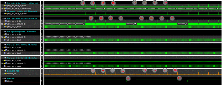
The guidelines previously outlined for normal (Four Channel) operation mode also apply to Single Channel operation mode, where each block/segment Aurora data transfer must still begin with a Block Control Word, end with the DMDLOAD_REQ, and conform to the 300ns setup time requirement. However, there is one major difference regarding the APPS FPGA and DLPC964 Controller handshaking in this mode. The actual DMD operation triggered by the DMDLOAD_REQ only corresponds to what is sent with segment 0. BLKLOADZ is not asserted for segments 3, 2 and 1. (Figure 7-10 for details).
All four segments of the selected data block must be operated in the correct order, otherwise the DLPC964 controller does not carry out the proper DMD operation to that block.
 Figure 7-10 Single Channel Operation
Waveform Example
Figure 7-10 Single Channel Operation
Waveform Example- Apps Aurora Data Transfer for DMD Block 0 in Single Channel Mode:
- 1A—Block Control Word, DMD data, and DMDLOAD_REQ for DMD block 0 Segment 3
- 1B—Block Control Word, DMD data, and DMDLOAD_REQ for DMD block 0 Segment 2
- 1C—Block Control Word, DMD data, and DMDLOAD_REQ for DMD block 0 Segment 1
- 1D—Block Control Word, DMD data, and DMDLOAD_REQ for DMD block 0 Segment 0
- 1E—Segment 0 DMDLOAD_REQ triggers DLPC964 Controller to begin block 0 data loading. BLKLOADZ is asserted to indicate the operation is in process.
- Apps Aurora Data Transfer for DMD Block 1 in Single Channel Mode:
- 2A—Block Control Word, DMD data, and DMDLOAD_REQ for DMD block 1 Segment 3
- 2B—Block Control Word, DMD data, and DMDLOAD_REQ for DMD block 1 Segment 2
- 2C—Block Control Word, DMD data, and DMDLOAD_REQ for DMD block 1 Segment 1
- 2D—Block Control Word, DMD data, and DMDLOAD_REQ for DMD block 1 Segment 0
- 2E—Segment 0 DMDLOAD_REQ triggers DLPC964 Controller to begin block 1 data loading. BLKLOADZ is asserted to indicate the operation in process.