JAJST20 March 2024 DLPC964
PRODUCTION DATA
- 1
- 1 特長
- 2 アプリケーション
- 3 概要
- 4 Pin Configuration and Functions
- 5 Specifications
-
6 Detailed Description
- 6.1 Overview
- 6.2 Functional Block Diagram
- 6.3 Feature Description
- 6.4
Device Functional
Modes
- 6.4.1 DLPC964 Aurora 64B/66B Input Data and Command Write Cycle
- 6.4.2 DMD Row Operation
- 6.4.3 Block Load Address Select
- 6.4.4 Block Mode Select
- 6.4.5 Mirror Clocking Pulse (MCP)
- 6.5
Register Map
- 6.5.1
Register Table Overview
- 6.5.1.1 FPGA_INTERRUPT_STATUS Register
- 6.5.1.2 FPGA_INTERRUPT_ENABLE_CONTROL Register
- 6.5.1.3 FPGA_MAIN_STATUS Register
- 6.5.1.4 FPGA_VERSION Register
- 6.5.1.5 FPGA_MAIN_CTRL Register
- 6.5.1.6 SELF_TEST_REG Register
- 6.5.1.7 DMDIF_ERROR_STATUS_CLR Register
- 6.5.1.8 DMDIF_ERROR_STATUS Register
- 6.5.1.9 PRBS7_MACRO0_TEST_RESULT Register
- 6.5.1.10 PRBS7_MACRO1_TEST_RESULT Register
- 6.5.1.11 PRBS7_MACRO2_TEST_RESULT Register
- 6.5.1.12 PRBS7_MACRO3_TEST_RESULT Register
- 6.5.1.13 PRBS7_TEST_CONTROL Register
- 6.5.1.14 PRBS7_TEST_RUNSTATUS Register
- 6.5.1.15 LS_BUS_TEST_RESULT Register
- 6.5.1.16 DMD_TYPE Register
- 6.5.1.17 HSS_RESET Register
- 6.5.1.18 HSS_CHANNEL_STATUS Register
- 6.5.1.19 HSS_LANE_STATUS Register
- 6.5.1.20 HSS_CH0_SOFTERROR_COUNT Register
- 6.5.1.21 HSS_CH1_SOFTERROR_COUNT Register
- 6.5.1.22 HSS_CH2_SOFTERROR_COUNT Register
- 6.5.1.23 HSS_CH3_SOFTERROR_COUNT Register
- 6.5.1.24 HSS_SOFTERROR_COUNT_RESET Register
- 6.5.1.25 HSSI_Channel_0_DMD_Data_GT_Cell_Control Register
- 6.5.1.26 HSSI_Channel_0_DMD_Clock_GT_Cell_Control Register
- 6.5.1.27 HSSI_Channel_1_DMD_Data_GT_Cell_Control Register
- 6.5.1.28 HSSI_Channel_1_DMD_Clock_GT_Cell_Control Register
- 6.5.1.29 HSSI_Channel_2_DMD_Data_GT_Cell_Control Register
- 6.5.1.30 HSSI_Channel_2_DMD_Clock_GT_Cell_Control Register
- 6.5.1.31 HSSI_Channel_3_DMD_Data_GT_Cell_Control Register
- 6.5.1.32 HSSI_Channel_3_DMD_Clock_GT_Cell_Control Register
- 6.5.1.33 HSSI_DMD_Vcm_Value Register
- 6.5.1.34 TEST_DMD_ID Register
- 6.5.1.35 TEST_DMD_FUSE1 Register
- 6.5.1.36 TEST_DMD_FUSE2 Register
- 6.5.1.37 TEST_DMD_FUSE3 Register
- 6.5.1.38 TEST_DMD_FUSE4 Register
- 6.5.1
Register Table Overview
-
7 Application and Implementation
- 7.1 Application Information
- 7.2 Typical Application
- 7.3 Interfacing to DLPC964 Controller High Speed Serial (HSS) Aurora 64B/66B Inputs
- 7.4 Power Supply Recommendations
- 7.5 Layout
- 7.6 Layout Example
- 8 Device and Documentation Support
- 9 Revision History
- 10Mechanical, Packaging, and Orderable Information
7.3.1.3 DMDLOAD_REQ Setup Time Requirement
The APPS FPGA user logic can assert the DMDLOAD_REQ signal as soon as the Aurora block data transfer is complete, as long as it is at least 300ns after sending the first data packet of that block data transfer. This setup time requirement is due to the 300ns transmit latency of the Aurora TX/RX channel paths, and guarantees the DLPC964 Controller will receive the DMDLOAD_REQ flag after the arrival of Aurora block data transfer.
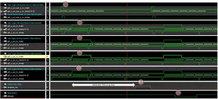
In most cases, this 300ns setup requirement is naturally met due to the size of a data block transfer. It is large enough to guarantee well over 300ns from the first valid data packet being sent to the last ones of a block when the APPS FPGA can assert the DMDLOAD_REQ signal. The 300ns setup window becomes critical when the APPS FPGA attempts to send a small partial DMD data block such as in Figure 7-7, showing an example of the APPS FPGA sending a total of just 3 rows (Table 7-3, ROW_LENGTH = 3) of a DMD partial data block to the DLPC964 Controller:
APPS FPGA transmits a Block Control Word to indicate the start of an Aurora block data transfer.
After sending 3 rows of data through the four Aurora data interface channels, the APPS FPGA waits for the 300ns setup time to expire before issuing a DMDLOAD_REQ. Note, 300ns is measured from the start of the first TVALID on the data interface.
Once the setup time has been met, the APPS FPGA asserts DMDLOAD_REQ.
BLKLOADZ is asserted by the DLPC964 Controller, indicating a DMD data load operation is in progress.
 Figure 7-7 Example of DMDLOAD_REQ Setup
Time for Three DMD Row Load Operation.
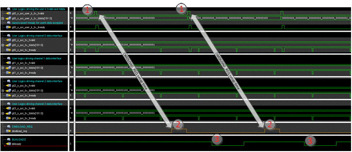
 For operations that do not require a data packet, such as block-clear (Table 7-3, LOAD_TYPE = 001) and block-set (Table 7-3, LOAD_TYPE = 010), the 300ns setup time for DMDLOAD_REQ is still required and is measured from the Block Control Word packet. An example of block-set operation is described in Figure 7-8:
- APPS FPGA transmits a Block Control Word packet to start a block-set operation. Notice that this operation does not require any block data, and the four Aurora data interfaces stay idle (gtX_s_axi_tx_tvalid = ‘0’).
- APPS FPGA asserts a DMDLOAD_REQ after the 300ns setup time. 300ns is measured from the Block Control Word, because the block-set operation does not require any Aurora data block transfer.
- DLPC964 Controller asserts BLKLOADZ, indicating block-set operation is in progress.
 Figure 7-8 Example of DMDLOAD_REQ Setup
Time for Block Set Operation.