JAJSEV0G july 2016 – august 2023 DP83822H , DP83822HF , DP83822I , DP83822IF
PRODUCTION DATA
- 1
- 1 特長
- 2 アプリケーション
- 3 概要
- 4 Revision History
- 5 Device Comparison Table
- 6 Pin Configuration and Functions
-
7 Specifications
- 7.1 Absolute Maximum Ratings
- 7.2 ESD Ratings
- 7.3 Recommended Operating Conditions
- 7.4 Thermal Information
- 7.5 Electrical Characteristics
- 7.6 Timing Requirements, Power-Up Timing
- 7.7 Timing Requirements, Power-Up With Unstable XI Clock
- 7.8 Timing Requirements, Reset Timing
- 7.9 Timing Requirements, Serial Management Timing
- 7.10 Timing Requirements, 100 Mbps MII Transmit Timing
- 7.11 Timing Requirements, 100 Mbps MII Receive Timing
- 7.12 Timing Requirements, 10 Mbps MII Transmit Timing
- 7.13 Timing Requirements, 10 Mbps MII Receive Timing
- 7.14 Timing Requirements, RMII Transmit Timing
- 7.15 Timing Requirements, RMII Receive Timing
- 7.16 Timing Requirements, RGMII
- 7.17 Normal Link Pulse Timing
- 7.18 Auto-Negotiation Fast Link Pulse (FLP) Timing
- 7.19 10BASE-Te Jabber Timing
- 7.20 100BASE-TX Transmit Latency Timing
- 7.21 100BASE-TX Receive Latency Timing
- 7.22 Timing Diagrams
- 7.23 Typical Characteristics
-
8 Detailed Description
- 8.1 Overview
- 8.2 Functional Block Diagram
- 8.3 Feature Description
- 8.4
Device Functional Modes
- 8.4.1 MAC Interfaces
- 8.4.2
Serial Management Interface
- 8.4.2.1 Extended Register Space Access
- 8.4.2.2 Write Address Operation
- 8.4.2.3 Read Address Operation
- 8.4.2.4 Write (No Post Increment) Operation
- 8.4.2.5 Read (No Post Increment) Operation
- 8.4.2.6 Write (Post Increment) Operation
- 8.4.2.7 Read (Post Increment) Operation
- 8.4.2.8 Example Write Operation (No Post Increment)
- 8.4.2.9 Example Read Operation (No Post Increment)
- 8.4.3 100BASE-TX
- 8.4.4 100BASE-FX
- 8.4.5 10BASE-Te
- 8.4.6 Auto-Negotiation (Speed / Duplex Selection)
- 8.4.7 Auto-MDIX Resolution
- 8.4.8 Loopback Modes
- 8.4.9 BIST Configurations
- 8.4.10 Cable Diagnostics
- 8.4.11 Fast Link Down Functionality
- 8.5 Programming
- 8.6 Register Maps
- 9 Application and Implementation
- 10Power Supply Recommendations
- 11Layout
- 12Device and Documentation Support
- 13Mechanical, Packaging, and Orderable Information
パッケージ・オプション
デバイスごとのパッケージ図は、PDF版データシートをご参照ください。
メカニカル・データ(パッケージ|ピン)
- RHB|32
サーマルパッド・メカニカル・データ
発注情報
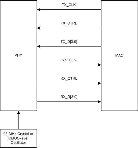
8.4.1.3 Reduced Gigabit Media Independent Interface (RGMII)
The DP83822 also supports Reduced Gigabit Media Independent Interface (RGMII) as specified by RGMII version 2.0. RGMII is designed to reduce the number of pins required to connect the MAC and PHY. To accomplish this goal, the control signals are multiplexed. Both rising and falling edges of the clock are used to sample the control signal pin on the transmit and receive paths. For 10-Mbps operation, RX_CLK and TX_CLK operate at 2.5 MHz. For 100-Mbps operation, RX_CLK and TX_CLK operate at 25 MHz.
The RGMII signals are summarized below:
| FUNCTION | PINS |
|---|---|
| Data Signals | TX_D[3:0] |
| RX_D[3:0] | |
| Transmit and Receive Signals | TX_CTRL |
| RX_CTRL |
 Figure 8-7 RGMII Signaling
During packet reception, RX_CLK may be stretched on either the positive or negative pulse to accommodate the transition from the internal free running clock to a recovered clock (data synchronous). Additionally, when the speed of the PHY changes, a similar clock stretching of the positive or negative pulses is allowed to prevent clock glitches. Data may be duplicated on the falling edge of the clock because double data rate (DDR) is only required for 1-Gbps operation, which is not supported by the DP83822.
The DP83822 supports in-band status indication. To help simplify detection of link status, speed and duplex, the DP83822 provides inter-frame signals on RX_D[3:0] pins as specified in Table 8-5 below.
| RX_DV | RX_D3 | RX_D[2:1] | RX_D0 |
|---|---|---|---|
| 0 Note: In-band status only valid when RX_DV is low | Duplex Status: 1 = Full-Duplex 0 = Half-Duplex | RX_CLK Clock Speed: 00 = 2.5-MHz (10 Mbps) 01 = 25-MHz (100 Mbps) 10 = Reserved 11 = Reserved | Link Status: 1 = Valid link established 0 = Link not established |