JAJSEV0G july 2016 – august 2023 DP83822H , DP83822HF , DP83822I , DP83822IF
PRODUCTION DATA
- 1
- 1 特長
- 2 アプリケーション
- 3 概要
- 4 Revision History
- 5 Device Comparison Table
- 6 Pin Configuration and Functions
-
7 Specifications
- 7.1 Absolute Maximum Ratings
- 7.2 ESD Ratings
- 7.3 Recommended Operating Conditions
- 7.4 Thermal Information
- 7.5 Electrical Characteristics
- 7.6 Timing Requirements, Power-Up Timing
- 7.7 Timing Requirements, Power-Up With Unstable XI Clock
- 7.8 Timing Requirements, Reset Timing
- 7.9 Timing Requirements, Serial Management Timing
- 7.10 Timing Requirements, 100 Mbps MII Transmit Timing
- 7.11 Timing Requirements, 100 Mbps MII Receive Timing
- 7.12 Timing Requirements, 10 Mbps MII Transmit Timing
- 7.13 Timing Requirements, 10 Mbps MII Receive Timing
- 7.14 Timing Requirements, RMII Transmit Timing
- 7.15 Timing Requirements, RMII Receive Timing
- 7.16 Timing Requirements, RGMII
- 7.17 Normal Link Pulse Timing
- 7.18 Auto-Negotiation Fast Link Pulse (FLP) Timing
- 7.19 10BASE-Te Jabber Timing
- 7.20 100BASE-TX Transmit Latency Timing
- 7.21 100BASE-TX Receive Latency Timing
- 7.22 Timing Diagrams
- 7.23 Typical Characteristics
-
8 Detailed Description
- 8.1 Overview
- 8.2 Functional Block Diagram
- 8.3 Feature Description
- 8.4
Device Functional Modes
- 8.4.1 MAC Interfaces
- 8.4.2
Serial Management Interface
- 8.4.2.1 Extended Register Space Access
- 8.4.2.2 Write Address Operation
- 8.4.2.3 Read Address Operation
- 8.4.2.4 Write (No Post Increment) Operation
- 8.4.2.5 Read (No Post Increment) Operation
- 8.4.2.6 Write (Post Increment) Operation
- 8.4.2.7 Read (Post Increment) Operation
- 8.4.2.8 Example Write Operation (No Post Increment)
- 8.4.2.9 Example Read Operation (No Post Increment)
- 8.4.3 100BASE-TX
- 8.4.4 100BASE-FX
- 8.4.5 10BASE-Te
- 8.4.6 Auto-Negotiation (Speed / Duplex Selection)
- 8.4.7 Auto-MDIX Resolution
- 8.4.8 Loopback Modes
- 8.4.9 BIST Configurations
- 8.4.10 Cable Diagnostics
- 8.4.11 Fast Link Down Functionality
- 8.5 Programming
- 8.6 Register Maps
- 9 Application and Implementation
- 10Power Supply Recommendations
- 11Layout
- 12Device and Documentation Support
- 13Mechanical, Packaging, and Orderable Information
パッケージ・オプション
デバイスごとのパッケージ図は、PDF版データシートをご参照ください。
メカニカル・データ(パッケージ|ピン)
- RHB|32
サーマルパッド・メカニカル・データ
発注情報
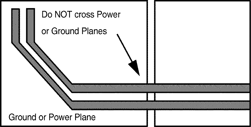
11.1.2 Return Path
A general best practice is to have a solid return path beneath all signal traces. This return path can be a continuous ground or DC power plane. Reducing the width of the return path can potentially affect the impedance of the signal trace. This effect is more prominent when the width of the return path is comparable to the width of the signal trace. Breaks in return path between the signal traces should be avoided at all cost. A signal crossing a split plane may cause unpredictable return path currents and could impact signal quality and result in emissions issues.
 Figure 11-2 Differential Signal Pair and Plane Crossing