JAJSID0G december 2019 – july 2023 DP83826E , DP83826I
PRODUCTION DATA
- 1
- 1 特長
- 2 アプリケーション
- 3 概要
- 4 Revision History
- 5 Mode Comparison Tables
- 6 Pin Configuration and Functions (ENHANCED Mode)
- 7 Pin Configuration and Functions (BASIC Mode)
- 8 Specifications
-
9 Detailed Description
- 9.1 Overview
- 9.2 Functional Block Diagram
- 9.3
Feature Description
- 9.3.1 Auto-Negotiation (Speed/Duplex Selection)
- 9.3.2 Auto-MDIX Resolution
- 9.3.3 Energy Efficient Ethernet
- 9.3.4 EEE for Legacy MACs Not Supporting 802.3az
- 9.3.5 Wake-on-LAN Packet Detection
- 9.3.6 Low Power Modes
- 9.3.7 RMII Repeater Mode
- 9.3.8 Clock Output
- 9.3.9 Media Independent Interface (MII)
- 9.3.10 Reduced Media Independent Interface (RMII)
- 9.3.11 Serial Management Interface
- 9.3.12 100BASE-TX
- 9.3.13 10BASE-Te
- 9.3.14 Loopback Modes
- 9.3.15 BIST Configurations
- 9.3.16 Cable Diagnostics
- 9.3.17 LED and GPIO Configuration
- 9.4 Programming
- 9.5 Register Maps
- 10Application and Implementation
- 11Power Supply Recommendations
- 12Layout
- 13Device and Documentation Support
- 14Mechanical, Packaging, and Orderable Information
パッケージ・オプション
メカニカル・データ(パッケージ|ピン)
- RHB|32
サーマルパッド・メカニカル・データ
- RHB|32
発注情報
9.3.16.2 Fast Link-Drop Functionality
The DP83826 includes advanced link-drop capabilities that support various real-time applications. The link-drop mechanism is configurable and includes enhanced modes that allow extremely fast link-drop reaction times.
The DP83826 supports an enhanced link-drop mechanism, also called fast link-drop (FLD), which shortens the observation window for determining link. There are multiple ways of determining link status, which can be enabled or disabled based on user preference.
Depending on what mode the DP83826 is in, the default state of FLD will differ. In ENHANCED mode, FLD and all its detection mechanisms are disabled by default through pulling down Strap7. For EtherCAT applications or applications with Fast link drop enabled and expect to handle Baseline wander packets, it is recommended to disable signal energy detect, which can be done by setting Strap8. The table below summarizes the modes enabled by strap.
| Strap Configuration | RX Error Count | MLT3 Error Count | Low SNR Threshold | Signal/Energy Loss | Descrambler Link Loss |
|---|---|---|---|---|---|
(Default) Strap7 = LOWStrap1 = X Strap8 = X | Disabled | Disabled | Disabled | Disabled | Disabled |
| Strap7 = HIGH Strap1 = HIGH Strap8 = LOW | Enabled | Enabled | Enabled | Enabled | |
| Strap7 = HIGH Strap1 = LOW Strap8 = LOW | Enabled | Disabled | Enabled | Disabled | |
| Strap7 = HIGH Strap1 = LOW Strap8 = HIGH | Enabled | Disabled | Disabled | Disabled |
In BASIC mode, fast link-drop is enabled by default. The default mechanisms in BASIC mode will be RX error and signal/energy loss.
In both modes, FLD can be configured using the Control Register #3 (CR3, register address 0x000B). Bits[3:0] and bit[10] allow for various FLD conditions to be enabled. When link-drop occurs, indication of a particular fault condition can be read from the Fast Link Drop Status Register (FLDS, register address 0x000F).
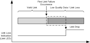
 Figure 9-8 Fast Link-Drop
Fast link-drop criteria include:
- RX error count - when a predefined number of 32 RX_ERs occur in a 10-μs window, the link is dropped.
- MLT3 error count - when a predefined number of 20 MLT3 errors occur in a 10-μs window, the link is dropped. To use the MLT3 error based FLD, please configure register Fast Link Drop Config Register 1 (FLDCFG1, register address 0x0117) to 0x0417.
- Low SNR threshold - when a predefined number of 20 threshold crossings occur in a 10-μs window, the link is dropped.
- Signal/energy loss - when the energy detector indicates energy loss, the link is dropped.
- Descrambler link loss - when the Descrambler loses lock, the link is dropped. To use the Descrambler link loss based FLD, please configure bits[5:0] of Fast Link Drop Config Register 2 (FLDCFG2, register address 0x0131) to 0x08.
The fast link-drop functionality allows the use of each of these options separately or in any combination.