SNLS266E May 2007 – March 2015 DP83848C , DP83848I , DP83848VYB , DP83848YB
PRODUCTION DATA.
- 1Introduction
- 2Revision History
- 3 Device Comparison
-
4Pin Configuration and Functions
- 4.1 Pin Layout
- 4.2 Package Pin Assignments
- 4.3 Serial Management Interface
- 4.4 Mac Data Interface
- 4.5 Clock Interface
- 4.6 LED Interface
- 4.7 JTAG Interface for DP83848I/VYB/YB
- 4.8 Reset and Power Down
- 4.9 Strap Options
- 4.10 10 Mb/s and 100 Mb/s PMD Interface
- 4.11 Special Connections
- 4.12 Power Supply Pins
- 5Specifications
-
6Detailed Description
- 6.1 Overview
- 6.2 Functional Block Diagram
- 6.3 Feature Description
- 6.4 Device Functional Modes
- 6.5
Programming
- 6.5.1
Architecture
- 6.5.1.1 100BASE-TX Transmitter
- 6.5.1.2
100BASE-TX Receiver
- 6.5.1.2.1 Analog Front End
- 6.5.1.2.2 Digital Signal Processor
- 6.5.1.2.3 Signal Detect
- 6.5.1.2.4 MLT-3 to NRZI Decoder
- 6.5.1.2.5 NRZI to NRZ
- 6.5.1.2.6 Serial to Parallel
- 6.5.1.2.7 Descrambler
- 6.5.1.2.8 Code-group Alignment
- 6.5.1.2.9 4B/5B Decoder
- 6.5.1.2.10 100BASE-TX Link Integrity Monitor
- 6.5.1.2.11 Bad SSD Detection
- 6.5.1.3
10BASE-T Transceiver Module
- 6.5.1.3.1 Operational Modes
- 6.5.1.3.2 Smart Squelch
- 6.5.1.3.3 Collision Detection and SQE
- 6.5.1.3.4 Carrier Sense
- 6.5.1.3.5 Normal Link Pulse Detection/Generation
- 6.5.1.3.6 Jabber Function
- 6.5.1.3.7 Automatic Link Polarity Detection and Correction
- 6.5.1.3.8 Transmit and Receive Filtering
- 6.5.1.3.9 Transmitter
- 6.5.1.3.10 Receiver
- 6.5.1
Architecture
- 6.6
Memory
- 6.6.1
Register Block
- 6.6.1.1
Register Definition
- 6.6.1.1.1 Basic Mode Control Register (BMCR)
- 6.6.1.1.2 Basic Mode Status Register (BMSR)
- 6.6.1.1.3 PHY Identifier Register #1 (PHYIDR1)
- 6.6.1.1.4 PHY Identifier Register #2 (PHYIDR2)
- 6.6.1.1.5 Auto-Negotiation Advertisement Register (ANAR)
- 6.6.1.1.6 Auto-Negotiation Link Partner Ability Register (ANLPAR) (BASE Page)
- 6.6.1.1.7 Auto-Negotiation Link Partner Ability Register (ANLPAR) (Next Page)
- 6.6.1.1.8 Auto-Negotiate Expansion Register (ANER)
- 6.6.1.1.9 Auto-Negotiation Next Page Transmit Register (ANNPTR)
- 6.6.1.2
Extended Registers
- 6.6.1.2.1 PHY Status Register (PHYSTS)
- 6.6.1.2.2 MII Interrupt Control Register (MICR)
- 6.6.1.2.3 MII Interrupt Status and Misc. Control Register (MISR)
- 6.6.1.2.4 False Carrier Sense Counter Register (FCSCR)
- 6.6.1.2.5 Receiver Error Counter Register (RECR)
- 6.6.1.2.6 100 Mb/s PCS Configuration and Status Register (PCSR)
- 6.6.1.2.7 RMII and Bypass Register (RBR)
- 6.6.1.2.8 LED Direct Control Register (LEDCR)
- 6.6.1.2.9 PHY Control Register (PHYCR)
- 6.6.1.2.10 10 Base-T Status/Control Register (10BTSCR)
- 6.6.1.2.11 CD Test and BIST Extensions Register (CDCTRL1)
- 6.6.1.2.12 Energy Detect Control (EDCR)
- 6.6.1.1
Register Definition
- 6.6.1
Register Block
- 7Application, Implementation, and Layout
- 8Device and Documentation Support
- 9Mechanical, Packaging, and Orderable Information
7 Application, Implementation, and Layout
NOTE
Information in the following applications sections is not part of the TI component specification, and TI does not warrant its accuracy or completeness. TI’s customers are responsible for determining suitability of components for their purposes. Customers should validate and test their design implementation to confirm system functionality.
7.1 Application Information
The device is a physical layer Ethernet transceiver. Typical operating voltage is 3.3 V with power consumption less than 270 mW. When using the device for Ethernet application, it is necessary to meet certain requirements for normal operation of device. Following typical application and design requirements can be used for selecting appropriate component values for DP83848.
7.2 Typical Application
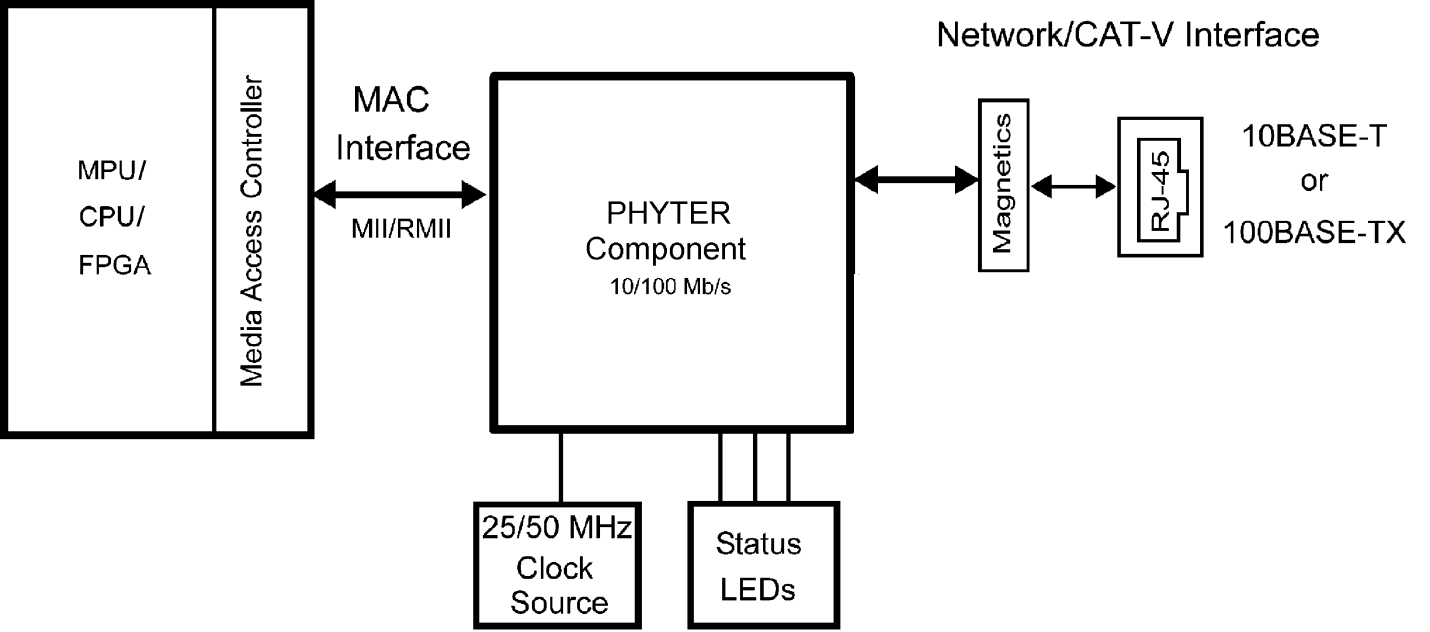 Figure 7-1 Typical Application Schematic
7.2.1 Design Requirements
The design requirements for DP83848 are:
- Vin = 3.3 V
- Vout = Vcc – 0.5 V
- Clock Input = 25 MHz for MII and 50 MHz for RMII
7.2.1.1 TPI Network Circuit
Figure 7-2 shows the recommended circuit for a 10/100 Mb/s twisted pair interface. To the right is a partial list of recommended transformers. It is important that the user realize that variations with PCB and component characteristics requires that the application be tested to ensure that the circuit meets the requirements of the intended application.
- Pulse H1102
- Pulse H2019
- Pulse J0011D21
- Pulse J0011D21B
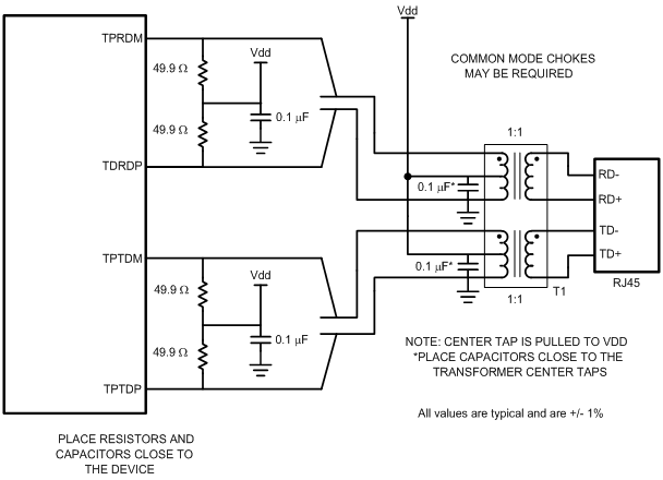 Figure 7-2 10/100 Mb/s Twisted Pair Interface
7.2.1.2 Clock IN (X1) Requirements
The DP83848VYB supports an external CMOS level oscillator source or a crystal resonator device.
7.2.1.2.1 Oscillator
If an external clock source is used, X1 should be tied to the clock source and X2 should be left floating.
Specifications for CMOS oscillators: 25 MHz in MII Mode and 50 MHz in RMII Mode are listed in Table 7-1 and Table 7-2.
7.2.1.2.2 Crystal
A 25-MHz, parallel, 20-pF load crystal resonator should be used if a crystal source is desired. Figure 7-4 shows a typical connection for a crystal resonator circuit. The load capacitor values will vary with the crystal vendors; check with the vendor for the recommended loads.
The oscillator circuit is designed to drive a parallel resonance AT cut crystal with a minimum drive level of 100 mW and a maximum of 500 µW. If a crystal is specified for a lower drive level, a current limiting resistor should be placed in series between X2 and the crystal.
As a starting point for evaluating an oscillator circuit, if the requirements for the crystal are not known, CL1 and CL2 should be set at 33 pF, and R1 should be set at 0 Ω.
Specification for 25-MHz crystal are listed in Table 7-3.
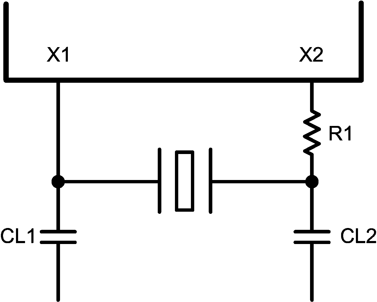 Figure 7-3 Crystal Oscillator Circuit
Table 7-1 25-MHz Oscillator Specification
| PARAMETER | CONDITION | MIN | TYP | MAX | UNIT |
|---|---|---|---|---|---|
| Frequency | 25 | MHz | |||
| Frequency Tolerance | Operational Temperature | ±50 | ppm | ||
| Frequency Stability | 1 year aging | ±50 | ppm | ||
| Rise / Fall Time | 20% - 80% | 6 | nsec | ||
| Jitter | Short term | 800(1) | psec | ||
| Jitter | Long term | 800(1) | psec | ||
| Symmetry | Duty Cycle | 40% | 60% |
Table 7-2 50-MHz Oscillator Specification
| PARAMETER | CONDITION | MIN | TYP | MAX | UNIT |
|---|---|---|---|---|---|
| Frequency | 50 | MHz | |||
| Frequency Tolerance | Operational Temperature | ±50 | ppm | ||
| Frequency Stability | Operational Temperature | ±50 | ppm | ||
| Rise / Fall Time | 20% - 80% | 6 | nsec | ||
| Jitter | Short term | 800(1) | psec | ||
| Jitter | Long term | 800(1) | psec | ||
| Symmetry | Duty Cycle | 40% | 60% |
Table 7-3 25-MHz Crystal Specification
| PARAMETER | CONDITION | MIN | TYP | MAX | UNIT |
|---|---|---|---|---|---|
| Frequency | 25 | MHz | |||
| Frequency Tolerance | Operational Temperature | ±50 | ppm | ||
| Frequency Stability | 1 year aging | ±50 | ppm | ||
| Load Capacitance | 25 | 40 | pF |
7.2.1.3 Power Feedback Circuit
To ensure correct operation for the DP83848VYB, parallel caps with values of 10 µF and 0.1 µF should be placed close to pin 23 (PFBOUT) of the device.
Pin 18 (PFBIN1), pin 37 (PFBIN2), pin 23 (PFBIN3) and pin 54 (PFBIN4) must be connected to pin 31 (PFBOUT), each pin requires a small capacitor (.1 µF). See Figure 7-4 below for proper connections.
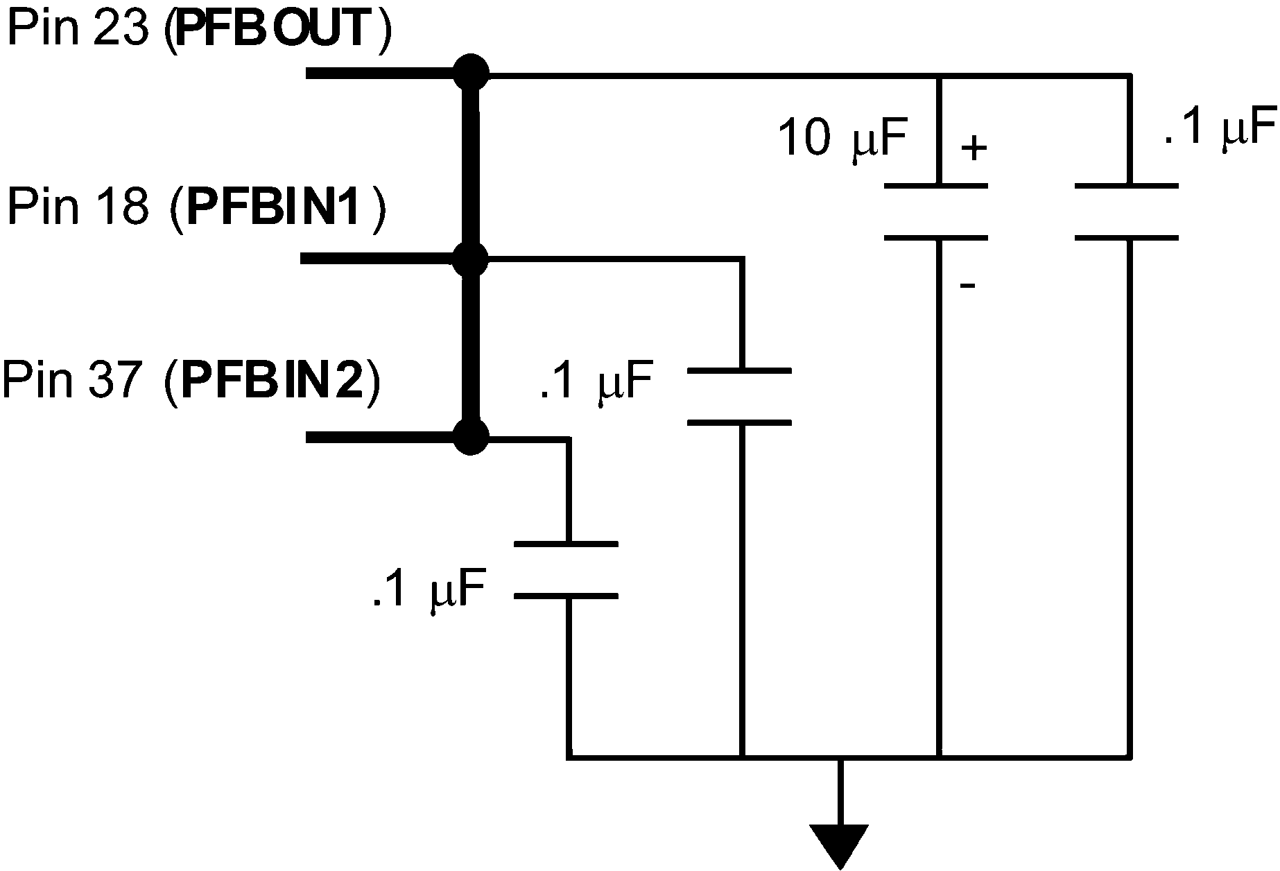 Figure 7-4 Power Feedback Connection
7.2.1.3.1 Power Down and Interrupt
The Power Down and Interrupt functions are multiplexed on pin 7 of the device. By default, this pin functions as a power-down input and the interrupt function is disabled. Setting bit 0 (INT_OE) of MICR (0x11h) will configure the pin as an active low interrupt output.
7.2.1.3.1.1 Power Down Control Mode
The PWRDOWN_INT pins can be asserted low to put the device in a Power Down mode. This is equivalent to setting bit 11 (Power Down) in the Basic Mode Control Register, BMCR (0x00h). An external control signal can be used to drive the pin low, overcoming the weak internal pullup resistor. Alternatively, the device can be configured to initialize into a Power Down state by use of an external pulldown resistor on the PWRDOWN_INT pin. Since the device will still respond to management register accesses, setting the INT_OE bit in the MICR register will disable the PWRDOWN_INT input, allowing the device to exit the Power Down state.
7.2.1.3.1.2 Interrupt Mechanisms
The interrupt function is controlled through register access. All interrupt sources are disabled by default. Setting bit 1 (INTEN) of MICR (0x11h) will enable interrupts to be output, dependent on the interrupt mask set in the lower byte of the MISR (0x12h). The PWRDOWN_INT pin is asynchronously asserted low when an interrupt condition occurs. The source of the interrupt can be determined by reading the upper byte of the MISR. One or more bits in the MISR will be set, denoting all currently pending interrupts. Reading of the MISR clears ALL pending interrupts.
Example: To generate an interrupt on a change of link status or on a change of energy detect power state, the steps would be:
- Write 0003h to MICR to set INTEN and INT_OE
- Write 0060h to MISR to set ED_INT_EN and LINK_INT_EN
- Monitor PWRDOWN_INT pin
When PWRDOWN_INT pin asserts low, the user would read the MISR register to see if the ED_INT or LINK_INT bits are set, for example, which source caused the interrupt. After reading the MISR, the interrupt bits should clear and the PWRDOWN_INT pin will deassert.
7.2.1.4 Magnetics
The magnetics have a large impact on the PHY performance as well. While several components are listed below, others may be compatible following the requirements listed in Table 6-4. It is recommended that the magnetics include both an isolation transformer and an integrated common mode choke to reduce EMI. When doing the layout, do not run signals under the magnetics. This could cause unwanted noise crosstalk. Likewise void the planes under discrete magnetics, this will help prevent common mode noise coupling. To save board space and reduce component count, an RJ-45 with integrated magnetics may be used.
Table 7-4 Magnetics Requirements
| PARAMETER | TYP | UNITS | CONDITION |
|---|---|---|---|
| Turn Ratio | 1:1 | — | ±2% |
| Insertion Loss | -1 | dB | 1-100 MHz |
| Return Loss | -16 | dB | 1-30 MHz |
| -12 | dB | 30-60 MHz | |
| 10 | dB | 60-80 MHz | |
| Differential to Common Rejection Ratio | -30 | dB | 1-50MHz |
| -20 | dB | 50-150 MHz | |
| Crosstalk | -35 | dB | 30 MHz |
| -30 | dB | 60 MHz | |
| Isolation | 1,500 | Vrms | HPOT |
7.2.1.5 ESD Protection
Typically, ESD precautions are predominantly in effect when handling the devices or board before being installed in a system. In those cases, strict handling procedures need be implemented during the manufacturing process to greatly reduce the occurrences of catastrophic ESD events. After the system is assembled, internal components are less sensitive from ESD events.
See Section 5.2 for ESD rating.
7.2.2 Detailed Design Procedure
7.2.2.1 MAC Interface (MII/RMII)
The Media Independent Interface (MII) connects the PHYTER component to the Media Access Controller (MAC). The MAC may in fact be a discrete device, integrated into a microprocessor, CPU or FPGA. On the MII signals, the IEEE specification states the bus should be 68-Ω impedance. For space critical designs, the PHYTER family of products also support Reduced MII (RMII). For additional information on this mode of operation, refer to the AN-1405 DP83848 Single 10/100 Mb/s Ethernet Transceiver Reduced Media Independent Interface (RMII) Mode Application Report (SNLA076).
7.2.2.1.1 Termination Requirement
To reduce digital signal energy, 50-Ω series termination resistors are recommended for all MII output signals (including RXCLK, TXCLK, and RX Data signals.)
7.2.2.1.2 Recommended Maximum Trace Length
Although RMII and MII are synchronous bus architectures, there are a number of factors limiting signal trace lengths. With a longer trace, the signal becomes more attenuated at the destination and thus more susceptible to noise interference. Longer traces also act as antennas, and if run on the surface layer, can increase EMI radiation. If a long trace is running near and adjacent to a noisy signal, the unwanted signals could be coupled in as cross talk. It is recommended to keep the signal trace lengths as short as possible. Ideally, keep the traces under 6 inches. Trace length matching, to within 2.0 inches on the MII or RMII bus is also recommended. Significant differences in the trace lengths can cause data timing issues. As with any high speed data signal, good design practices dictate that impedance should be maintained and stubs should be avoided throughout the entire data path.
7.2.2.2 Calculating Impedance
The following equations can be used to calculate the differential impedance of the board. For microstrip traces, a solid ground plane is needed under the signal traces. The ground plane helps keep the EMI localized and the trace impedance continuous. Since stripline traces are typically sandwiched between the ground/supply planes, they have the advantage of lower EMI radiation and less noise coupling. The trade off of using strip line is lower propagation speed.
7.2.2.2.1 Microstrip Impedance - Single-Ended

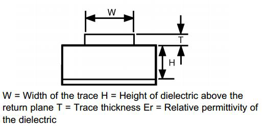 Figure 7-5 Microstrip Impedance - Single-Ended
7.2.2.2.2 Stripline Impedance – Single Ended

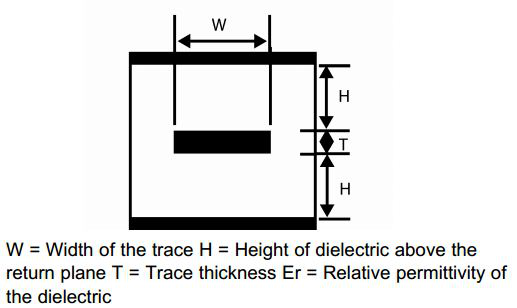 Figure 7-6 Stripline Impedance – Single Ended
7.2.2.2.3 Microstrip Impedance - Differential

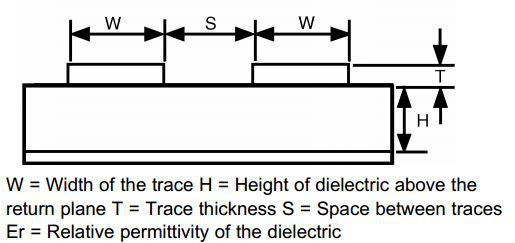 Figure 7-7 Microstrip Impedance - Differential
7.2.2.2.4 Stripline Impedance - Differential

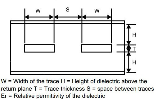 Figure 7-8 Stripline Impedance - Differential
7.2.3 Application Curves
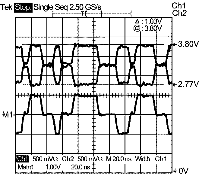 Figure 7-9 Sample 100 Mb/s Waveform (MLT-3)
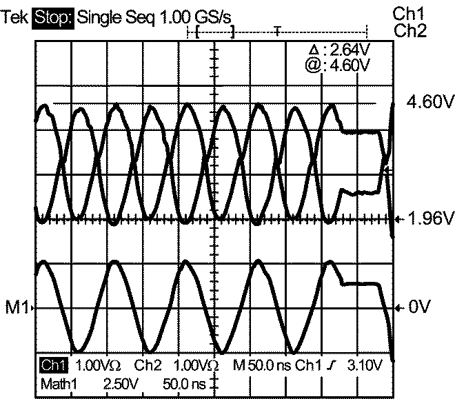 Figure 7-10 Sample 10 Mb/s Waveform
7.3 Layout
7.3.1 Layout Guidelines
7.3.1.1 PCB Layout Considerations
Place the 49.9-Ω,1% resistors and 0.1-μF decoupling capacitor near the PHYTER TD± and RD± pins and via directly to the Vdd plane.
Stubs should be avoided on all signal traces, especially the differential signal pairs. See Figure 7-11. Within the pairs (for example, TD+ and TD-) the trace lengths should be run parallel to each other and matched in length. Matched lengths minimize delay differences, avoiding an increase in common mode noise and increased EMI. See Figure 7-11.
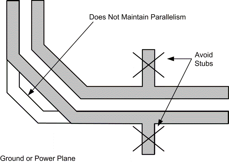 Figure 7-11 Differential Signal Pair – Stubs
Ideally, there should be no crossover or via on the signal paths. Vias present impedance discontinuities and should be minimized. Route an entire trace pair on a single layer if possible.
PCB trace lengths should be kept as short as possible.
Signal traces should not be run such that they cross a plane split. See Figure 7-12. A signal crossing a plane split may cause unpredictable return path currents and would likely impact signal quality as well, potentially creating EMI problems.
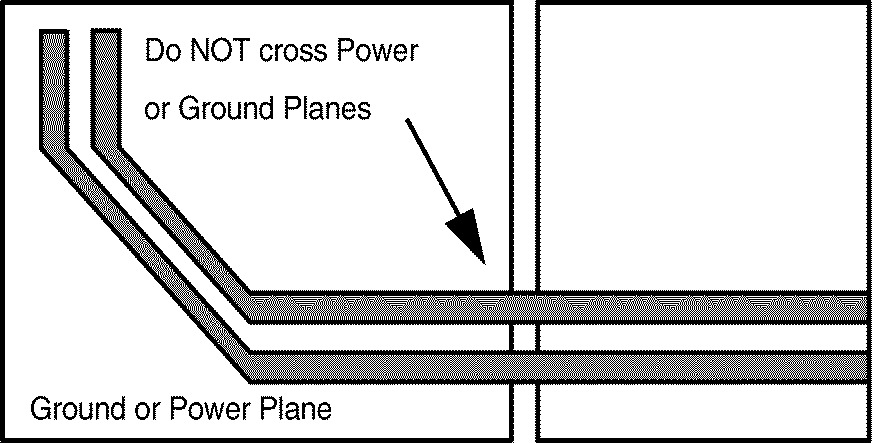 Figure 7-12 Differential Signal Pair-Plane Crossing
MDI signal traces should have 50 Ω to ground or 100 Ω differential controlled impedance. Many tools are available online to calculate this.
7.3.1.2 PCB Layer Stacking
To meet signal integrity and performance requirements, at minimum a four layer PCB is recommended for implementing PHYTER components in end user systems. The following layer stack-ups are recommended for four, six, and eight-layer boards, although other options are possible.
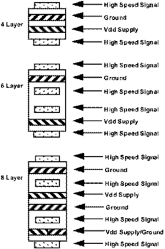 Figure 7-13 PCB Stripline Layer Stacking
Within a PCB it may be desirable to run traces using different methods, microstrip vs. stripline, depending on the location of the signal on the PCB. For example, it may be desirable to change layer stacking where an isolated chassis ground plane is used. Figure 7-14 illustrates alternative PCB stacking options.
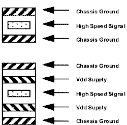 Figure 7-14 Alternative PCB Stripline Layer Stacking
7.3.2 Layout Example
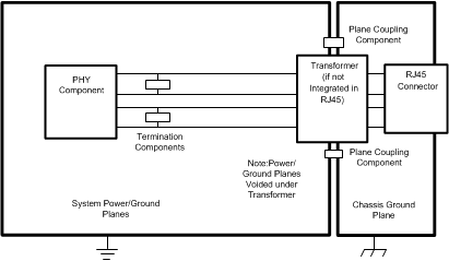 Figure 7-15 Layout Example
7.4 Power Supply Recommendations
The device Vdd supply pins should be bypassed with low impedance 0.1-μF surface mount capacitors. To reduce EMI, the capacitors should be places as close as possible to the component Vdd supply pins, preferably between the supply pins and the vias connecting to the power plane. In some systems it may be desirable to add 0-Ω resistors in series with supply pins, as the resistor pads provide flexibility if adding EMI beads becomes necessary to meet system level certification testing requirements. (See Figure 6.8) It is recommended the PCB have at least one solid ground plane and one solid Vdd plane to provide a low impedance power source to the component. This also provides a low impedance return path for non-differential digital MII and clock signals. A 10.0-μF capacitor should also be placed near the PHY component for local bulk bypassing between the Vdd and ground planes.
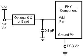 Figure 7-16 Vdd Bypass Layout